

In the constantly evolving technology landscape, the demand for innovative solutions that address modern challenges in security, communication and imaging has reached unprecedented levels. As industries look to solutions that improve efficiency, safety and scalability, the terahertz (THz) band has emerged as a viable option. Positioned between the microwave and infrared spectra, the THz frequency band possesses properties that enable advancements across multiple domains. Figure 1 shows the THz frequency band and where it resides in the electromagnetic spectrum, along with some popular applications.
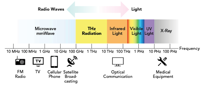
Figure 1 The electromagnetic spectrum. Source: Canon.
THz waves, characterized by their ability to penetrate a variety of materials, non-ionizing nature and high-resolution imaging capabilities, present an opportunity to transform how industries address solutions to complex problems. The application of THz technology spans a wide array of fields, from real-time security screening to next-generation wireless communication and advanced medical diagnostics. This article explores THz light source technology developed by Canon, along with the applications and the broader implications of the adoption of this fundamental technology across industries. It will also highlight the challenges and opportunities associated with commercializing THz technology, offering insights into its future trajectory and impact. The technology is available for licensing or acquisition to enable broader commercial applications and Canon is partnering with yet2, a global technology scouting and innovation firm, to commercialize this technology.
THE SCIENCE OF THZ WAVES
THz radiation spans frequencies between 0.1 and 10 THz in the electromagnetic spectrum. This range bridges the gap between the microwave and infrared regions. This frequency band is attracting substantial development attention and activity because it offers properties that are advantageous for a multitude of applications.
Key Characteristics of THz Waves
Non-Ionizing Nature: Unlike X-rays, THz radiation is non-ionizing, meaning it does not have enough energy to remove tightly bound electrons from atoms. This makes THz waves inherently safer for applications involving human interaction, such as medical imaging and security scanning.
Material Penetration: THz waves can penetrate materials like fabric, paper and certain plastics. This capability is an important differentiator in applications such as security screening, where non-invasive detection of concealed items is crucial. Additionally, THz waves are absorbed by water and other liquids, enabling precise identification of substances.
Spectral Fingerprinting: The interaction of THz waves with materials produces unique absorption and reflection patterns, known as spectral fingerprints. These patterns enable the identification and differentiation of materials at a molecular level, making THz waves invaluable for applications in chemical analysis and quality control.
Wavelength and Resolution: With wavelengths shorter than mmWaves but longer than infrared, THz waves strike a balance that offers higher-resolution imaging capabilities. This property is particularly useful in applications requiring detailed visualization, such as non-destructive testing and medical diagnostics.
The ability of THz waves to interact with a wide range of materials stems from their intermediate position in the electromagnetic spectrum. THz waves are reflected by metallic surfaces, allowing for the identification of metallic objects in security settings. Also helpful in security applications, THz radiation is highly absorbed by water. This enables the detection of liquid substances, which is crucial for identifying hazardous liquids. These high frequency THz waves scatter when interacting with powders, providing a non-invasive means to analyze the composition of granular materials.
When compared to the adjacent mmWave and infrared regions of the spectrum, THz waves offer a unique combination of benefits. Even though mmWave frequencies and equipment are widely used in security scanners, THz frequencies and equipment provide more resolution. Additionally, mmWave frequencies do not have the penetration capabilities of THz wave in certain materials. Infrared radiation provides high-resolution imaging, but it is susceptible to scattering and absorption in specific environments, particularly those with high moisture content. The net result is that THz waves offer greater versatility for these and other applications.
EMERGING SCIENTIFIC RESEARCH
There is a significant amount of ongoing research into the THz spectrum and the possibilities. Scientists are exploring advanced methods to enhance the generation and detection of THz radiation, along with devices. Some of the more prominent areas of exploration include:
Quantum Cascade Lasers: These devices promise efficient and compact THz wave generation for portable applications.
Plasmonics: This field involves generating, detecting and manipulating light at metal/dielectric interfaces at nanoscale dimensions. Leveraging surface plasmon resonances to improve the interaction of THz waves with materials is being investigated to enable higher sensitivity in sensors.
Metamaterials: Metamaterials are being investigated for a variety of applications. In the THz frequency range, engineered structures that manipulate THz waves in novel ways are being developed with the goal of enabling applications like cloaking and ultra-high-resolution imaging.
The science of THz signals and the ongoing research are intertwined. These areas highlight the current capabilities of the technology and underscore the potential for future innovation. As research progresses, the boundaries of what is possible with THz technology will continue to expand, driving advancements across multiple fields.
THZ LIGHT SOURCE DEVELOPMENT

Figure 2 Canon THz light source. Source: Canon.
To help crystalize the potential of THz waves into reality, Canon has introduced the semiconductor-based THz light source shown in Figure 2. The THz light source uses a resonant tunnel diode (RTD) manufactured on indium phosphide (InP) in an active array antenna structure. InP is a III-V compound semiconductor material like gallium arsenide (GaAs). While GaAs has been a mainstay technology for mmWave applications, InP has higher electron mobility and a wider bandgap, making this technology increasingly attractive for higher frequency applications. InP is also a direct bandgap material, which allows for more efficient light emission and absorption. The direct bandgap makes the material compatible with optical components and suitable for integration into optical networks.