

On-wafer S-parameter measurement can be achieved by establishing a signal connection channel between the vector network analyzer (VNA) and the wafer through a probe station. Before 2010, the development of on-wafer S-parameter measurement technologies was relatively slow in China and it had been using existing foreign technologies for a long time. In the past 10 years, China has been catching up in this field and continuously narrowing the gap with the rest of the world. China has been gradually completing the localization of calibration methods, wafer probes and on-wafer calibration standards from RF to terahertz frequencies to develop the metrological capability of on-wafer S-parameter measurement equipment. This article introduces the development of relevant technologies in this field, both domestically and internationally, which provides guidance for subsequent development.
With the development of semiconductor technology, MMICs are constantly evolving toward higher frequency bands and more challenging performance requirements are becoming common. As a result, the measurement accuracy requirements are becoming increasingly strict and new high-precision calibration methods are constantly emerging. Before 2020, all components required for S-parameter measurement were imported to China. In recent years, with the rapid development of the domestic semiconductor industry in China, the gap between on-wafer S-parameter measurement technology and capabilities between China and foreign counterparts has gradually narrowed and breakthroughs have been made in related technologies. Increasingly, key components for on-wafer measurement are being internally developed in China.
TECHNIQUES OUTSIDE CHINA
Typically, the on-wafer S-parameter measurement system consists of a VNA and frequency extender module, a probe station, microwave probes, on-wafer calibration standards and some ancillary components, as shown in Figure 1. On-wafer S-parameter measurement systems need to be calibrated before measurement.
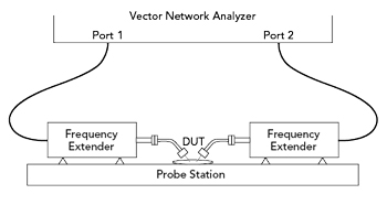
Figure 1 On-wafer S-parameter measurement system diagram.

Figure 2 (a) NIST on-wafer S-parameter calibration system. (b) Comparison results for maximum stable gain before and after crosstalk correction.
Regarding on-wafer S-parameter calibration from RF to terahertz, the National Institute of Standards and Technology (NIST) in the U.S. has always been in a leading position. NIST has considered the introduction of new error sources in the on-wafer S-parameter measurement systems in the terahertz frequency band compared to microwave and RF frequencies.1 Since 2013, research on calibration techniques for on-wafer S-parameters in the RF to terahertz frequency range has not stopped and the calibration frequency band has been raised from the previous limits of 110 GHz and 325 GHz to the current 1.1 THz. With funding from the U.S. Defense Advanced Research Projects Agency (DARPA), NIST proposed optimized multiline TRL2, a new calibration method for precise on-wafer S-parameters in the terahertz frequency band. They have also developed corresponding on-wafer calibration standards. This calibration method has achieved good results in transistor modeling in the frequency range below 325 GHz and enables continuous measurement for even higher accuracy. Figure 2a shows a photo of the on-wafer S-parameter measurement system established by NIST and Figure 2b shows the comparison results before and after coupling correction.
In August 2022, the U.S. government proposed the CHIPS and Science Act, which provides financial support and tax incentives for the domestic semiconductor industry through legislation. Meanwhile, NIST released the Strategic Opportunities for U.S. Semiconductor Manufacturing-Facilitating U.S. Leadership and Competitiveness through Advancements in Measurements and Standards based on the content of the CHIPS and Science Act. This document outlines seven major challenges facing the U.S. semiconductor industry as a priority development direction for the next five years. This includes “modeling and simulation of semiconductor materials, design and components,” which involves the importance and challenges of precise modeling of semiconductor chips at terahertz frequencies. In October 2023, NIST restarted its research on terahertz frequency metrology and measurement technology.
EU metrology institutions such as NPL in the U.K. and PTB in Germany closely follow the U.S. The EU supports 12 institutions, including NPL, PTB and MEATS in Switzerland, along with VSL in the Netherlands, to conduct EU-funded “Microwave Measurement of Planar Circuits and Components” project. The EU metrology agency has established an on-wafer S-parameter calibration system covering 110 to approximately 325 GHz and conducted calibration technology research in related fields. In terms of calibration algorithms, considering the existence of new error sources in the on-wafer S-parameter measurement system in the terahertz frequency band, the EU’s metrology technical agency recommends 16-term error model calibration3 to reduce measurement errors in on-wafer S-parameter measurement in the terahertz frequency band and improve the measurement accuracy. From 2019 to 2024, the European Association of National Metrology Institutions conducted traceability and validation work on the on-wafer S-parameters ranging from 100 GHz to 1.1 THz.4,5 Figure 3a shows the on-wafer S-parameter calibration system from NPL and Figure 3b shows the wafer calibration standards based on 16-term error models developed by PTB.

Figure 3 (a) On-wafer S-parameter calibration system from NPL. (b) On-wafer calibration standards based on 16-term error models developed by PTB.
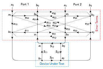
Figure 4 16-term error model including crosstalk error.
DOMESTIC CALIBRATION METHODS
For frequencies below 67 GHz, on-wafer calibration methods have matured in China and have been widely applied. These include short-open-load-through (SOLT),6 short-open-load-reciprocal (SOLR),7 line-reflect-reflect-match (LRRM)8 and through-reflect-line (TRL).9 In addition, some specialized on-wafer calibration methods have been developed for specific applications, such as the series resistor calibration method. The multiline TRL calibration method was first proposed by Marks10 to address the traceability of waveguide systems and has now been implemented in on-wafer S-parameters metrology.
However, the accuracy of the traditional calibration methods mentioned previously decreases with increasing frequency. The main reason is that the error model used in the calibration method cannot characterize the leakage between the probe ports, which is known as crosstalk. Crosstalk can occur for several reasons; it may result from the radiation of electromagnetic energy from the device under test (DUT), energy leakage between probe tips and energy leakage between substrates. To solve this problem, one technical approach is to use a 16-term error model calibration method with crosstalk errors, as shown in Figure 4 and other new calibration methods derived from the 16-term error model. Another approach is to use a parallel crosstalk error method with obvious physical significance, combined with the conventional waveguide port calibration and microwave probe extraction two-step calibration method, which has been applied in on-wafer systems.
The enhanced SOLR (eSOLR) calibration method11 uses an 8-term error model, shown in Figure 5 and includes e00, e11, e01, e10, e22, e33, e23 and e32. In the actual calibration process, only seven of the eight systematic error models need to be solved to complete the calibration. There are two processes for solving the eSOLR calibration algorithm. The first step is to solve the 6-term error model and the second is to solve the scale coefficient.
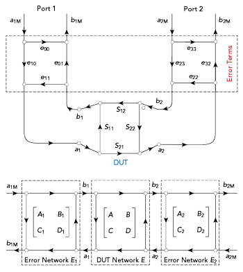
Figure 5 8-term error model and its simplified ABCD error network.
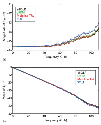
Figure 6 (a) S21 magnitude comparison for different calibration methods. (b) S21 phase comparison for different calibration methods.

Figure 7 Measurement results using different calibration methods.
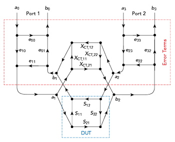
Figure 8 Error model for the calibration-on-the-fly method.
To facilitate the calculation, the eight basic error terms are expressed by the equivalent ABCD transfer matrix. The error network E1 corresponds to the error network composed of e00, e11, e01 and e10 and the error network E2 corresponds to the error network composed of e22, e33, e23 and e32. E1 and E2 contain parasitic parameters of the contact points of the DUT. The eSOLR calibration method provides the foundation for terahertz measurement by combining a straight-through transmission line standard that does not need to be defined, two pairs of reflection standards (open and short standard) and a pair of accurately-defined load standards to enable terahertz wafer calibration.