
The promises and shortcomings of microelectromechanical systems (MEMS) switch technology have become almost legendary. Perhaps no other electronic component in history has been the source of so much hype—and the cause of so much disillusionment. So much so, that Internet sites advise engineers to steer clear of MEMS switch technology. Fortunately for those who have patiently followed this technology, the troubling early days are finally over and MEMS switches are rapidly fulfilling all of their earlier promise. This article takes a fresh look at lessons learned and where things stand today, along with prospects for a bright future.
Past
The first MEMS electrical switch was announced by IBM nearly 30 years ago.1 Although the MEMS acronym was not coined for another decade,2 this was one of the first practical microelectromechanical devices that used semiconductor fabrication techniques to build small mechanical structures in silicon that were moved or “actuated” electrically. It also showed that MEMS could create an entirely new class of switch technology that combined the advantages of semiconductor manufacturing with the best features of electromechanical relays. In particular, it was predicted that MEMS switches would be small, have low power consumption and low loss—and, if properly manufactured in high volume, would be low cost and highly reliable.
The first part of this promise was realized by MEMS switch prototypes developed at leading US industrial research centers during the early 1990s.3 Work at Hughes Research Labs, Raytheon/Texas Instruments and the Rockwell Science Center clearly demonstrated that MEMS switches could be small and high performance, and that they could deliver bandwidth and linearity equal to or better than the best electromechanical relays. The only problem that (seemingly) remained to be solved was lifetime reliability, and the race was on.
When reliable commercial devices failed to quickly come out of Hughes, Raytheon and Rockwell, the door opened for other companies to enter the race and the level of development activity exploded. By the end of the 1990s, more than 100 companies and research institutions throughout the world had started MEMS switch development programs. Visible commercial activity peaked between 2000 and 2001 with product “pre-announcements” from a number of major manufacturers and the launch of multiple startup companies.4 Electrical performance was generally outstanding, but switch samples once again failed to meet customers’ expectations for quality and reliability.
The extensive wait of nearly 10 years for a viable MEMS switch product made customers wary of the difficulties involved in commercializing this technology. Although there were a number of good reasons for these failures (see Inset), the string of premature product announcements in 2000 and 2001 was the last straw. Customers became disillusioned by the hype surrounding MEMS switches and a cynical attitude toward the technology quietly settled into the marketplace. Driven by this serious case of market overexposure and a realization that hard proof of reliable product performance was the only way to successfully win customers, MEMS switch development moved into “stealth” mode after 2001. While much of this activity remains out of the public eye to this day, MEMS switch development efforts continue at some of the most prestigious companies throughout the world.
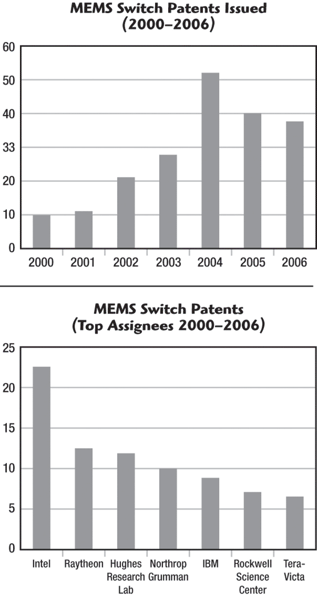
A basic search of MEMS switch and related patents issued after 2000 illustrates the breadth and depth of MEMS development. As shown in Figure 1, nearly 200 US patents were issued for MEMS switch-related technology in the last seven years alone. In addition to the early pioneers in MEMS switching, patent assignees include major MEMS component manufacturers (Agilent, Analog Devices and Freescale) and other leaders in the semiconductor industry (Intel, IBM, Samsung and Toshiba).

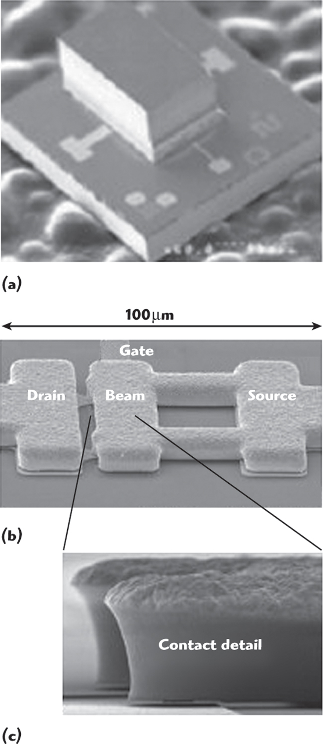
Despite the massive deployment of resources and expertise by industry leaders, the first commercial MEMS switch was introduced by a relatively small company. Initial demonstration of what would become the first commercial MEMS switch was reported in the late 1990s by a team from Northeastern University working in collaboration with Analog Devices. This technology was ultimately licensed by Radant MEMS, a Stow, MA, company that is focused on the production of high reliability switches for government and military applications. Radant MEMS announced the first DC to 10 GHz single-pole single-throw (SPST) MEMS switch able to meet 100 M cycles (see Figure 2) in 2004. The company has since introduced a single-pole double-throw (SPDT) switch that operates from DC to 20 GHz, and multi-contact series shunt switches that operate to 40 GHz.
The first commercially qualified MEMS switch was announced by TeraVicta Technologies in 2005 and began shipping in early 2006. Based on the company’s patented high force disk actuator (HFDA) technology (see Figure 3), the SPDT switch operates from DC to 7 GHz. TeraVicta led the industry by extending semiconductor qualification techniques to MEMS devices, and shipped the first-ever qualified commercial MEMS switch in early 2006. The company’s RF MEMS switches have found their way into high volume commercial applications including automatic test equipment, instrumentation and wireless communications.
Present
While a number of companies have disclosed either development efforts or limited sampling of advanced prototypes, at present only Radant MEMS and TeraVicta have MEMS switch products available in production quantities.5 Radant MEMS markets its products almost exclusively to government and military customers in the United States, while TeraVicta actively sells its products to commercial customers worldwide.
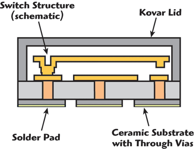
A discussion of the features of the TeraVicta MEMS switch provides a useful illustration of current MEMS switch technology. This switch uses a “device on package” construction with the switch built directly on a ceramic (alumina) wafer with conductive metal vias (see Figure 4). Individual switch features are patterned using conventional high volume semiconductor fabrication techniques, including sputter deposition and etching processes, with bulk metal layers fabricated via electroplating.
Device failures are minimized through the use of a proprietary high force disk actuator (HFDA), which provides substantial restoring force when the switch is in the closed position. This results in a very reliable operation, albeit at a relatively high switch voltage (68 V). Low voltage operation (3 to 5 V) is made possible through the use of a separate charge pump integrated circuit (IC). The package is completed by the attachment of a metal (Kovar) lid which provides a hermetic seal that eliminates the possibility of downstream contamination from backend manufacturing processes, and drastically reduces device failures due to contact contamination. The end result is a small (3.25 × 4.5 mm) surface-mountable micro-BGA ceramic package that provides a high efficiency, manufacturable electrical connection to the printed circuit board.
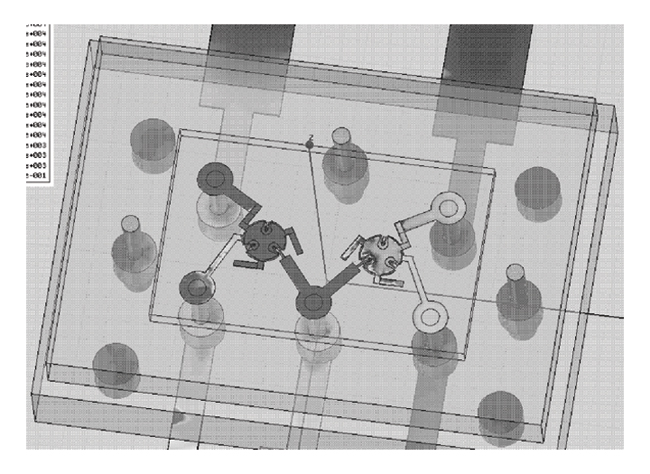
Switches with multiple contact configurations (SPDT, DPDT, etc.) can be constructed by connecting multiple HFDAs in a single package. This is illustrated by an RF electromagnetic/solid model of the basic DC to 7 GHz SPDT switch shown in Figure 5. The RF signal is conducted into the switch through a central terminal (RF common), which connects to two HFDAs on the device. Closing either HFDA results in an electrical connection to its respective output pin. Note that since the HFDAs can be independently actuated, it is possible to open (or close) both switch contacts at the same time or to arbitrarily control the opening and closing sequence of the switch contacts. Typical HFDA switches currently have a 70 µs switching speed.
The HFDA technology used by TeraVicta also provides resistance repeatability that is typically much better than 10 mW, which enables insertion loss reproducibility of better than 0.4 dB across the entire 7 GHz band. These switches are also rated for continuous operation at up to 15 W, with a peak power handling capability of at least 30 W.
By comparison, Radant MEMS uses a conventional silicon micromachining approach to produce a very high force cantilever switch structure, along with a wafer bonded hermetic package to insure hermeticity. Although the stiffness of this cantilever structure results in even higher operating voltages (90 V), switching times are reduced to 10 ms. Electrical connection is provided by wire bonding from the top surface of the chip to either a chip carrier or directly to the printed circuit board.
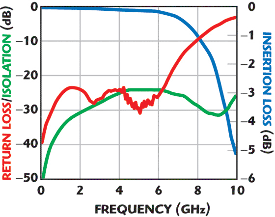
The characteristic RF performance of the TeraVicta DC to 7 GHz SPDT switch is shown in Figure 6. This MEMS switch delivers superior performance with insertion loss less than 0.1 dB at frequencies less than 1 GHz (0.4 dB at 7 GHz), with more than 20 dB of return loss and at least 25 dB of isolation. The simple construction of these switches also provides very low distortion for high power signals. Measured values of IP3 are typically in excess of 70 dBm, greater than the sensitivity of most measurement systems.
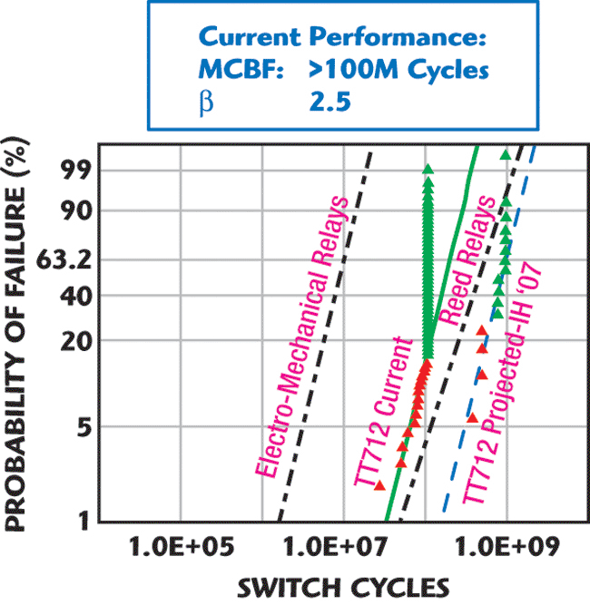
Although a number of MEMS switch developers have disclosed anecdotal results that show lifetimes of several billion cycles for individual switch samples, the perception of poor reliability still lingers in the marketplace. In response to this, TeraVicta has published lifetime data based on statistically significant samples of production devices.6 This data, reproduced in Figure 7, shows a Weibull plot of the failure distribution of current production devices. Included in the plot for comparison are representative failure distributions for competing electromechanical relays and reed relays. Additional data (green triangles) is included for devices that do not fail before 100 M cycles.
Device reliability in semiconductors and other electrical products is typically described in terms of mean time before failure or MTBF. The useful life of an RF MEMS switch is usually limited by the number of switch cycles, not by elapsed time, however, and their reliability is better described in terms of cycles before failure. Current MEMS switch products, manufactured by TeraVicta, have a typical switch life or mean cycles before failure (MCBF) of approximately 200 million cycles, 20 times higher than the best electromechanical relays.
Like other small electromechanical switches, MEMS switch lifetimes are significantly de-rated in hot switching applications (opening or closing the switch with voltage present) at power levels above 0 dBm. Hot switching at 1 V/1 mA, for example, currently degrades the expected operating life by approximately a factor of 10.
MEMS switch prices are currently competitive with alternative switch technologies, and average sale prices will continue to decrease as volume manufacturing increases, making MEMS switches a viable option for some of the most price-sensitive consumer applications. Today, most commercial applications take advantage of one or more of the unique features of these devices: small size, low (repeatable) loss, high linearity and broad bandwidth. Leading applications include high speed digital channel switching in automated test equipment, antenna switching in wireless communications and filter bank switching in instrumentation, military and aerospace applications.
Finally, it should be noted that a number of MEMS switch development activities are still underway at leading companies and research institutions worldwide. Switch prototypes have recently been announced by Omron, Panasonic, WiSpry and XCom Wireless. Sampling to select customers is reportedly underway. As of this writing, only Radant MEMS and TeraVicta have demonstrated the ability to deliver MEMS switches in production volume.5
Future
Three key trends will drive new applications for MEMS switches over the next three to five years: proliferation of a wide variety of new product configurations, substantial improvements in reliability, and significant reductions in switch size and cost.
The biggest change within the next year will be the emergence of a wide variety of new switch products. As an example, during 2007 TeraVicta will deploy its proven HFDA technology in a variety of new high performance high reliability MEMS switches. This includes the introduction of a new high frequency switch line with products operating across the DC to 36 GHz band, and a range of new multi-pole multi-throw switch configurations within the existing 7 GHz product family.
In coming years, new MEMS switch companies and/or new product features should also begin to emerge. Anticipated new product features include high isolation (> 45 dB) switches, isolated gate (four-terminal) operation for relay replacement applications, as well as significant improvements in hot switching performance. Although current charge pump ICs can be used to drive independent banks of MEMS switches, in the future direct integration of high voltage drivers with MEMS switches will enable the introduction of high reliability low voltage switches that eliminate the need for high voltage on the printed circuit board, a key feature for high volume consumer applications.
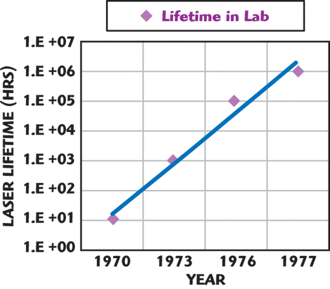
Substantial improvements in switch reliability will also occur over the next few years. The vast majority of field failures for MEMS switches today are caused by increases in contact resistance due to contamination of the switch contacts. Improvements in process cleanliness and package integrity, along with the elimination of contamination from other materials, will dramatically improve product lifetimes. Although a quantitative forecast of lifetime improvement is difficult, comparison with other emerging technologies can provide a qualitative guide. Similar requirements for process and materials improvement were faced by early developers of semiconductor diode lasers, for example. These researchers were able to consistently improve diode laser lifetime by a factor of 10 every 18 months (see Figure 8). A similar trend is likely for MEMS switches, with lifetimes of at least 10 B cycles and initial defect levels approaching 100 parts per million achieved over the next three to five years.
The most commercially significant trend over the next three to five years, however, will be reductions in switch size and cost. The substitution of lower cost materials, reductions in product size (proportional to cost) and higher fabrication utilization from increasing product sales will reduce product costs by a factor of 10 or more. Significant product size reductions will also occur, with packaged SPDT switches in form factors below 1.5 mm2 (a 90 percent size reduction).
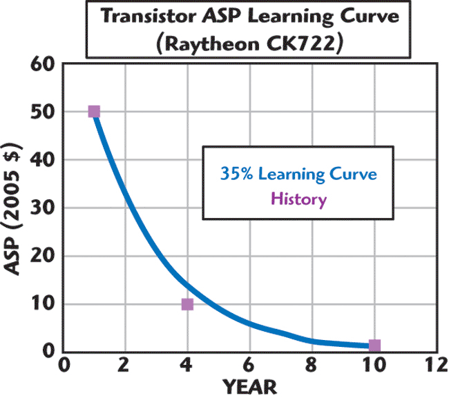
Although quantitative price forecasts are equally difficult, a review of historical price data from comparable technologies shows that most electronic devices experience a very uniform “learning curve,” with a 35 percent reduction per year in the average selling price (ASP) of a given function (transistor, gate, or instructions executed per second). The learning curve for the first high volume transistors, for example, is shown in Figure 9 (with prices adjusted to constant 2005 dollars). Although prices declined uniformly at the same rate of 35 percent per year, this analysis shows that the first transistors actually entered the market with a comparative unit price of $50. While there are reasons to suspect that limitations in size reduction will ultimately limit MEMS switch costs, price reductions of at least 35 percent per year are likely for the forseeable future. Already, MEMS switches are price competitive with existing switching solutions.
This fresh look at MEMS switch technology shows that despite lingering concerns about the reliability of this technology, a handful of MEMS switch manufacturers are finally delivering the first of a new family of high performance, high reliability switch products. These products are already finding high volume applications in automatic test equipment, instrumentation and communications. The list of applications is expected to explode as customers take advantage of all the benefits that MEMS switches have to offer.
References
- K.E. Petersen, “Micromechanical Membrane Switches on Silicon,” IBM Journal of Research and Development, Vol. 23, 1979, pp. 376–85.
- N. Maluf, An Introduction to Microelectromechanical Systems Engineering, Second Edition, Artech House, Norwood, MA, 2004.
- G.M. Rebeiz, RF MEMS: Theory, Design and Technology, John Wiley & Sons Inc., Hoboken, NJ, 2003.
- P. Chalmers, “Relay Races,” Mechanical Engineering-CIME, 1/1/2001.
- M. Potin, MEMS4Mobile 2006, Yole Developpement, 2006.
- J. McKillop, T. Fowler, D. Goins and R. Nelson, “Design, Performance and Qualification of a Commercially Available MEMS Switch,” Proceedings of the 2006 European Microwave Conference.
John McKillop received his BA degree in chemistry from Rice University and his PhD degree in chemistry from Stanford University. He held senior engineering and business development positions in a number of public companies and was a member of the research staff at IBM’s T.J. Watson Research Center. He has more than 20 years experience managing engineering, operations, business and technology development for companies focused on emerging technologies, particularly in the fields of MEMS, lasers and electro-optics. He has authored numerous publications, been invited to present on the applications for MEMS technology and taught multiple MEMS short courses. He is now vice president of product development and CTO at TeraVicta Technologies Inc.