

In today’s fast paced mobile handset market, design houses and manufacturers are challenged to meet a variety of targets to satisfy network provider’s high expectations in cellular and multimedia phones. Design cycle time, performance, feature requirements, form factor, quality and cost targets remain dominant selection criteria for mobile phone designers.
Next generation mobile multimedia applications (combining GSM/GPRS/EDGE/ WCDMA/WLAN/GPS in one phone, for example) put even more stringent requirements on the hardware architecture. Partitioning of the baseband and RF components are critical handset design decisions with respect to functionality, performance, integration level, size and cost.
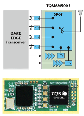
In an effort to lead the market trend in RF front-end architecture, integration and form factor size reduction, TriQuint Semiconductor has recently introduced its latest RF transmit (TX) module, the TQM6M5001, which adds full linear EDGE functionality to its successful family of 6 × 6 × 1.1 mm3 GSM/GPRS TX modules. This module family offers significant advantages in addressing these challenges using the TX module architecture already adopted with marketplace success by many GSM and EDGE phones.
TX modules in this family incorporate all of the critical RF transmit functions between the transceiver and the antenna into a single module offering a 60 percent size reduction compared to competing discrete solutions. EDGE operation has been added with no increase in size and has pin-out compatibility with the existing GSM/GPRS product, TQM6M4002, by re-using a ground pin as the EDGE (8PSK) mode pin. The high level integration needed to develop such an advanced product—adding functionality while keeping to the previous generation’s form factor—is possible by direct in-house control of key technologies including InGaP GaAs HBT and GaAs PHEMT circuits.
Key Design Advances
The new TQM6M5001 EDGE-enabled TX module builds on the discrete GSM/EDGE 850/900 and DCS1800/PCS1900 PA blocks and integrated power control found in present generation power amplifier modules. It adds a low insertion loss, quad-band PHEMT transmit/receive SP6T switch with four RX-ports, harmonic and low pass filtering, integrated switch decoder, and full ESD protection—all in an unprecedented size of 36 mm2. Full system level GSM/GPRS and EDGE compliance is assured when used with the latest generation of linear EDGE transceivers.
The TQM6M5001 EDGE TX module requires no external matching and eliminates the need to manage the PA-to-switch interface. This advancement in form factor and integration level was achieved in part by eliminating all surface-mount devices (SMD) inside the laminate-based module, resulting in clear size, cost and time-to-market advantages.
User Benefits and Process Technology
The TQM6M5001 transmit module combines the functionality of a quad-band power amplifier (PA) with power control, a low pass transmit filter (LPF), a quad-band TX/RX switch including decoder and ESD protection into one module (see Figure 1). A fundamental advantage of this transmit module is its built-in PA-to-front-end interface. By combining PA and antenna switch functionality into one module, the system bill of materials is significantly reduced, adding simplified supply chain management to an already lengthy list of advancements that benefit the mobile phone manufacturer.
In EDGE (8PSK) mode the module serves as a linear gain block with approximately 30 dB of gain in GSM850/900 and 34 dB of gain in the DCS/PCS bands, respectively. It provides a zero-bit, multi-bit or continuous bias feature for the lowest current consumption in 8PSK mode. The TQM6M5001 was designed utilizing in-house six-inch processes: InGaP GaAs HBT for the PA function and GaAs PHEMT for the LPF and switch components. All control functions for the PA and switch are incorporated into a proprietary CMOS design. A dedicated control pin toggles between GMSK and EDGE mode. All four switch RX ports are frequency independent allowing the user flexibility in handset phone-board layout.
Identical in size and pin-out to other GSM/GPRS TX module family members, the GMSK/EDGE-enabled TQM6M5001 is also laminate-based and uses bondwire inter-chip connections. All passive elements are integrated into the GaAs dies, thus eliminating the need for any SMDs inside the module. Full EDGE functionality could therefore be added to the module while maintaining a 6 × 6 × 1.1 mm3 footprint.
The TQM6M5001 transmit module architecture and interface is optimized for next generation multi-mode transceivers and baseband transceiver chip sets. By combining the TQM6M5001 GSM/EDGE TX module with TriQuint’s small form factor RX SAW filters (1.4 × 1.2 mm2 single filter series, or 2.0 × 1.5 mm2 2-in-1 filter series, for example) a complete RF solution is achieved with the assurance of full interface alignment and best-in-class RF performance.
Design Goals and Performance Highlights
A primary design goal met by the TQM6M5001 transmit module is full EDGE functionality and ETSI specification compliance in all four frequency bands (GSM850/900 and DCS1800/PCS1900) without compromising critical DC and RF performance in GSM/GPRS mode.
In GMSK mode, the maximum output power in the GSM850/900 band is typically 33.5 dBm with a system power-added efficiency (PAE) of 42 percent. In DCS/PCS band, a maximum output power of 31.5 dBm is achieved with a system PAE of 38 percent. For maximum output power, the harmonic power is less than –36 dBm in all frequency bands. The input power level range between +1 and +5 dBm is aligned to most transceivers currently available on the market. Ruggedness of the new transmit module exceeds a VSWR of 30:1 and stability is guaranteed up to a VSWR of 20:1, with all spurious signals below –36 dBm.
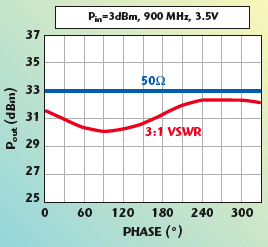
Mobile handset designs are typically calibrated at an output power of 33 dBm in the GSM850/900 band and at 30.5 dBm in the DCS/PCS (high) band. Since the impedance of the antenna can deviate from the nominal 50 Ω value depending on operational environment (for example, metal plane vs. human ear), network providers are more and more focused on the total radiated output power at the antenna. For a typical mismatch load (VSWR of 3:1), the peak-to-peak Pout variation of the TQM6M5001 vs. all phase angles is only 3 dB (see Figure 2). Therefore, the device is able to provide sufficient radiated output power even under widely varying operational conditions that the mobile phone might conceivably experience in daily use.
EDGE Performance
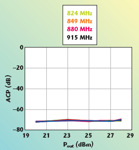
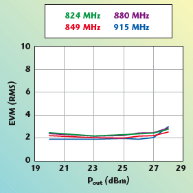
The TQM6M5001 transmit module behaves like a linear gain block in 8PSK mode. This means the output power of the TX module is controlled by the level of the input power. The transceiver provides the power setting and power ramp of the TX signal. For an output power of 27 dBm at the antenna pin, the ACPR at 400 kHz offset is typically lower than –65 dBc for nominal conditions (see Figure 3), and lower than –60 dBc for a minimum battery voltage of 3.2 V. EVM (RMS) performance is < 3 percent at the same output power level of 27 dBm showing full specification compliance with good margin (see Figure 4).
In EDGE (8PSK) mode the VRAMP pin is no longer used for setting the output power as was its function in GMSK mode. As previously noted the output power of the linear gain block is set by the input power as controlled by the transceiver. The VRAMP pin now serves as a bias control input in EDGE mode, setting the idle current (continuous bias) depending on the output power. By varying the applied voltage between 0.6 and 1.7 V, operating current can be adjusted as a function of output power to benefit from improved PAE at low output power levels.
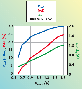
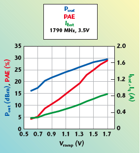
By utilizing this built-in feature of continuous bias in 8PSK mode, the current consumption at low output power can be improved significantly by re-adjusting the bias of the PA accordingly. The manufacturer has the option to use this feature in a multi-bit or continuous bias mode, or simply leave VRAMP constant for zero-bit operation. For example, at 1790 MHz, with a VRAMP voltage of 0.6 V, an output power up to 10 dBm can be achieved with an ACPR of < –58 dBc, thus resulting in an average operating current of 0.32A during an EDGE burst. With a control voltage of 1.7 V at the same Pout level the operating current would rise to approximately 0.75 A. More and more customers utilize this feature to their advantage as a current consumption benefit in next-generation handset designs.

Plots in Figure 5 and 6 illustrate PAE and Ibat as a function of VRAMP when optimized for an ACP400 of –58 dBc and shown at various output power settings (controlled by input power from the transceiver).
By design, full multi-slot GMSK/ EDGE capability is assured with the TQM6M5001 EDGE TX module as part of an RF system solution for today’s CMOS-based EDGE transceivers. Figure 7 shows full power vs. time specification compliance by the TQM6M5001 in the extreme case of a full power GMSK burst followed by the lowest power EDGE burst, as required by ETSI specifications.
Summary and Outlook
High level integration continues to set the pattern for succeeding generations of mobile phone RF front-end modules. As more functionality is added to advanced phone devices and handset form factors continue to shrink or grow slimmer, manufacturers expect RF module solutions that not only meet specifications, but pay dividends such as enhanced PAE, greater platform design facilitation and ease in generational transitioning that is inevitable as phones migrate from GSM/GPRS mode to full GPRS/EDGE, and beyond.
TriQuint has reached the next integration milestone with its 6 × 6 × 1.1 mm3 multi-mode GSM GPRS/ EDGE quad-band transmit module, the TQM6M5001, which offers mobile handset designers size and cost advantages to satisfy the high performance RF needs of next generation mobile handsets. Leveraging sophisticated in-house InGaP GaAs HBT and PHEMT GaAs processes with design expertise in power amplifiers, switches, signal filtering and CMOS design, TriQuint has successfully applied key processes and engineering skill sets to produce an RF transmit module with highly competitive performance and features.
With its EDGE functionality the TQM6M5001 is a significant step in the move toward fulfilling 3G RF radio and chipset concepts, which will further optimize the interface between transceiver and transmit modules across various modulation schemes. The successful implementation of cost-effective multi-mode phones will only be achievable if the combination of performance, cost, quality and form factor can be met in all respects. While the TQM6M5001 represents a significant contribution to the manufacture of new EDGE mobile phones, the company’s design engineers are already addressing the need for W-CDMA and EDGE (WEDGE) transmit modules that leverage existing experience in GSM, EDGE, W-CDMA and WLAN/ WiMAX PA and front-end modules to enable the next generation of 3G multimedia mobile handsets.
TriQuint Semiconductor Inc.,
Hillsboro, OR (503) 615-9000,
e-mail: info@tqs.com,
www.triquint.com.
RS No. 301