

As demonstrated in Figure 5(a), the two TPs can be controlled by keeping L1 constant and varying the value of W1. This process helps to determine an optimized bandwidth in the design. In Figure 5(b), reducing the value L1 from 278 to 218 μm results in the notch frequency shifting from 64 to 80 GHz. These results indicate that the frequency bandwidth of operation can be fully controlled in addition to the bandwidth. More importantly, the stopband attenuation level can also be optimized by adjusting the locations of the two TPs. Depending on the design specifications, the design trade-offs between high stopband attenuation and wide stopband bandwidth can be controlled by simply tuning these two variables.

Figure 5 EM simulation results sweeping W1 (a). EM simulation results sweeping L1 (b).
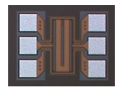
Figure 6 Die microphotograph of the designed dual-mode BSF.
MEASUREMENTS
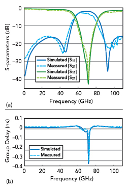
Figure 7 Measured S-parameters results for the dual-mode BSF (a). Measured group delay results for the dual-mode BSF (b).
To evaluate the performance of the presented dual-mode BSF, a prototype was fabricated in 0.13 μm SiGe technology. The die microphotograph is shown in Figure 6. Excluding the testing pads, the die size is only 0.11 × 0.248 mm. The S-parameter measurements were conducted with on-wafer ground-signal-ground (GSG) probes up to 110 GHz using an N5290A vector network analyzer from Keysight and 100 μm pitch GSG Infinity Probes with 1 mm connectors from FormFactor, Inc. The on-wafer calibration was made by using a conventional short-load-open-thru (SLOT) method to move the reference plane from the connectors of the equipment to the tips of the RF probes.
The simulated and measured power transmission and the group delay responses of the prototype are compared in Figure 7(a) and Figure 7(b). As observed, there is close agreement between predicted and experimental results. The minor discrepancies observed between simulated and measured power-reflection levels are attributed to the probes and GSG pads, which were not considered in the simulation process due to the increased computational cost.
Table 1 compares the results of this work to other similar efforts. As shown, this design has achieved the highest stopband attenuation and the widest stopband bandwidth while still maintaining a small footprint. These comparisons to other state-of-the-art designs demonstrate the overall performance improvement of the designed BSF.
CONCLUSION
An mmWave dual-mode BSF has been designed using 0.13 μm SiGe technology. The theoretical analysis of this design has been presented and validated through EM simulation. In addition, the fabricated BSF shows close agreement between EM simulation and measured results. These measured results show that the presented design has in-band suppression of more than 30 dB and low out-of-band insertion loss.

ACKNOWLEDGMENTS
This work is supported by the Southern Marine Science and Engineering Guangdong Laboratory (Zhanjiang) under contract No. ZJW-2019-04. This is a key project of Guangdong Province for promoting high-quality economic development (Marine Economic Development) in 2022: Research and development of key technology and equipment for Marine vibroseis system (GDNRC[2022]29).
References
- N. Mahmoud et al., “Compact size on-chip 60 GHz H-shaped resonator BPF,” IEEE Microwave and Wireless Components Letters, Vol. 26, No. 9, Sept. 2016, pp. 681–683.
- A. S. A. El-Hameed et al., “Ultracompact 60-GHz CMOS BPF employing broadside-coupled open-loop resonators,” IEEE Microwave and Wireless Components Letters, Vol. 27, No. 9, Sept. 2017, pp. 818–820.
- Z. Ge, L. Chen, R. Gómez-García and X. Zhu, “Millimeter-wave wide-band bandpass filter in CMOS technology using a two-layered highpass-type approach with embedded upper stopband,” IEEE Transactions on Circuits and Systems II: Express Briefs, Vol. 68 No. 5, May 2021, pp. 1586–1590.
- S. Chakraborty, Y. Yang, X. Zhu, O. Sevimli, Q. Xue, K. Esselle and M. Heimlich, “A broadside-coupled meander-line resonator in 0.13-μm SiGe technology for millimeter-wave application,” IEEE Electron Devices Letters, Vol. 37, No. 3, March 2016, pp. 329–331.
- Y. Yang, H. Zhu, X. Zhu and Q. Xue, “A low-loss bandpass filter using edge-coupled resonator with capacitive feeding in (Bi)-CMOS technology,” IEEE Electron Device Letters, Vol. 39 No. 6, June 2018, pp. 787–790.
- G. Bautista, H. Zhu, X. Zhu, Y. Yang, Y. Sun and E. Dutkiewicz, “Compact millimeter-wave bandpass filters using quasi-lumped elements in 0.13-μm (Bi)-CMOS technology for 5G wireless systems,” IEEE Transactions on Microwave Theory and Techniques, Vol. 67, No. 7, July 2019, pp. 3064–3073.
- H. Zhu, Y. Yang, X. Zhu, Y. Sun and S. W. Wong, “Miniaturized resonator and bandpass filter for silicon-based monolithic microwave and millimeter-wave integrated circuits,” IEEE Transactions on Circuits and Systems I: Regular Papers, Vol. 65, No. 12, Dec. 2018, pp. 4062–4071.
- L. S. Chen, et al., “A W-band SPDT switch with 15-dBm P1dB in 55- nm bulk CMOS,” IEEE Microwave and Wireless Components Letters, Vol. 32, No. 7, July. 2022, pp. 879–882.
- L. S. Chen et al., “A 90-GHz asymmetrical single-pole double-throw switch with <19.5-dBm 1-dB compression point in transmission mode using 55-nm bulk CMOS technology,” IEEE Transactions on Circuits and Systems I: Regular Papers, Vol. 68, No. 11, Nov. 2021, pp. 4616–4626.
- L. S. Chen, L. Chen, H. Zhu, R. Gómez -García and X. Zhu, “A wideband balanced amplifier using edge-coupled quadrature couplers in 0.13-μm SiGe HBT technology,” IEEE Transactions on Circuits and Systems I: Regular Papers, Early Access.
- S. Chakraborty et al., “A K-band frequency doubler with 35-dB fundamental rejection based on novel transformer balun in 0.13-μm SiGe technology,” IEEE Electron Device Letters, Vol. 37, No. 11, Nov. 2016, pp. 1375–1377.
- S. Chakraborty et al., “Analysis and comparison of Marchand and transformer baluns applied in GaAs,” IEEE Transactions on Circuits and Systems II: Express Briefs, Vol. 69, No. 11, 2022 pp. 4278–4282.
- S. Chakraborty et al., “An edge-coupled Marchand balun with partial ground for excellent balance in 0.13-μm SiGe technology,” IEEE Transactions on Circuits and Systems II: Express Briefs, Vol. 68, No. 1, Jan. 2021, pp. 226–230.
- L. Gao and G. M. Rebeiz, “Wideband bandpass filter for 5G millimeter-wave application in 45-nm CMOS silicon-on-insulator,” IEEE Electron Device Letters, Vol. 42, No. 8, August 2021, pp. 1244–1247.
- Z. Ge, L. Chen, L. Yang, R. Gómez -García and X. Zhu, “On-chip millimeter-wave integrated absorptive bandstop filter in (Bi)-CMOS technology,” IEEE Electron Device Letters, Vol. 42, No. 1, Jan. 2021, pp. 114–117.
- S. K. Thapa, R. K. Pokharel, B. Chen and A. Barakat, “On-chip Millimeter-Wave DGS based Bandstop Filter in 0.18-μm CMOS Process,” IEEE Transactions on Circuits and Systems II: Express Briefs, Vol. 69, No. 6, June 2022, pp. 2732–2736.
- V. Narayana Rao Vanukuru and V. Krishna Velidi, “Millimeter-wave CMOS 30/80 GHz sharp-rejection dual-band bandstop filters using TFMS open-stepped-impedance resonators,” IEEE Transactions on Circuits and Systems. II: Express Briefs, Vol. 68, No. 1, Jan. 2021, pp. 201–205.
- L. Chen, H. Zhu, R. Gómez -García and Xi Zhu, “Miniaturized on-chip notch filter with sharp selectivity and >35-dB attenuation in 0.13-μm bulk CMOS technology,” IEEE Electron Device Letters, Vol. 43, No. 8, 2022, pp.1175–1178.