

A compact mmWave on-chip dual-mode bandstop filter (BSF) is proposed and implemented in this work. The proposed BSF is realized with a broadside-coupled electromagnetic (EM) structure. Using this structure enables dual-mode operation, which helps to increase the attenuation bandwidth and the stopband attenuation level. As practical validation, a 72 GHz on-chip BSF is implemented in 0.13 μm SiGe technology and tested. There is close agreement between simulated and measured results for this on-chip BSF circuit. The measurement results show that the attenuation is better than 10 dB from 60 to 79 GHz, with 40 dB attenuation recorded at the optimized frequency. The passband insertion loss is better than 2.2 dB from DC to 50 GHz and 90 to 110 GHz. Excluding the pads, the size of the designed BSF is only 0.027 mm2.
On-chip passive components operating at mmWave frequencies are critical building blocks that can be found in many wireless systems, ranging from motion detection radar to high speed wireless data transmission. In particular, the compact passive components implemented in low-cost, silicon-based technology, including both CMOS and SiGe, are the ones that have drawn the most attention in the past few years.1-7 These passive components, like filters, baluns and couplers can be used as standalone building blocks or they can be co-designed with transistor circuits to further enhance the performance of active components.8-13
For filter design, the primary focus is on bandpass filters (BPFs). Although many novel EM structures have been presented for BPF design in the literature,1-7,14 the works that address the design issues related to BSF are limited. In addition, most of the previously published BSF works address narrowband applications.15-18 Another issue of on-chip mmWave BSF designs is the limited in-band attenuation that can be achieved, with attenuation levels of more than 30 dB desirable. This is difficult to achieve using the existing approaches, resulting in a knowledge gap when it comes to effectively designing a wideband on-chip BSF. In this paper, an innovative EM structure is proposed that takes advantage of dual-mode operation to increase the stopband bandwidth and attenuation of the designed BSF.
SIMPLIFIED CIRCUIT MODEL USING LUMPED ELEMENTS
To understand the proposed dual-mode BSF design concept, this section will present a theoretical analysis. A simplified circuit model using ideal lumped elements is given in Figure 1. This model is composed of two pairs of inductors with a value of L1 with a mutual inductance of M and multiple capacitors with capacitances of C1, C2 and C3. To investigate the transmitting characteristics of the device, the even- and odd-mode analysis method can be applied. The even- and odd-mode equivalent circuits are displayed in Figure 2(a) and Figure 2(b), respectively.
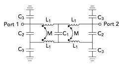
Figure 1 LC-equivalent circuit of the dual-mode BSF.
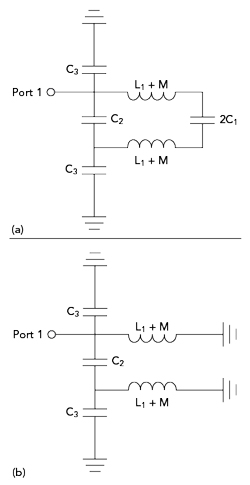
Figure 2 Even-mode LC-equivalent circuit (a) and odd-mode LC-equivalent circuit (b).
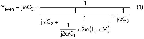
For the even-mode circuit, the input admittance can be expressed as:
For the odd-mode circuit, the input admittance can be expressed as:

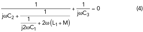
To create transmission poles (TPs) at the two edges of the stopband, the following equations should be satisfied:

By solving equations (3) and (4), the positions of TP1 and TP2 are located at:
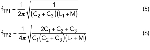
When the resonators are fixed, the positions of the TPs are affected by the mutual capacitance between the two inductors, which also determines the bandwidth of the stopband. Figure 3 shows the calculated S-parameters of three different cases. The first case is a notch filter with no mutual inductance between the two inductors. In this case, only one zero is realized at the center frequency without any TPs at two edges (in green). The second and third cases represent a dual-mode BSF with two TPs at two edges and the bandwidth of the stopband can be controlled in a certain range.
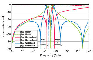
Figure 3 Synthesized S-parameters of a notch filter, a narrowband BSF and a wideband BSF.
Figure 4 3D view of the BSF EM structure (a). 2D view of the BSF EM structure with physical dimensions (b). Note: W1 = 26 mm, W2 = 4 mm, W3 = 10 mm, W4 = 10 mm and L1 = 248 mm.
IMPLEMENTATION OF THE DESIGNED BSF
The lumped-element model presented in Figure 1 is implemented using a 0.13 μm SiGe technology. This process provides seven metal layers, including two thick aluminum layers shown as TM1 and TM2 in Figure 4(a). These two layers are isolated by an SiO2 layer that has a dielectric constant of 4.1 and a thickness of 3 μm. The thickness of these two aluminum layers are 3 μm and 2 μm, respectively. In this design, these two metal layers are extensively used to construct the core of the BSF. The lower layer metals are thin and mainly used as the ground reference. The 2D view of the designed BSF is shown in Figure 4(b). This figure shows the adjustable dimensions of the bandstop filter design. To demonstrate that the designed bandwidth and stopband attenuation can be effectively controlled, a parametric study was conducted using EMX, an EM simulation tool from Cadence. Although multiple physical parameters can be used to control the performance, only two parameters were chosen in this study to limit the analysis to a reasonable length.