
Early discussions of the capabilities that will enable 6G envision materials and devices operating above 100 GHz. Indium phosphide (InP) is one semiconductor technology with the characteristics to achieve the required speed, efficiency and output power for sub-THz frequencies. To serve global wireless markets, InP process technology must be commercialized to maintain the performance advantages while able to be mass produced at the requisite prices to meet market needs. To develop InP into a mature technology, imec is researching nano-ridge engineering to grow InP on Si. Then, to integrate all the semiconductor components into a multi-function communications circuit, imec is exploring printed circuit board (PCB), 2.5D and 3D packaging technologies.
Every 10 years heralds a new generation of mobile communications. Over the generations, the number of subscribers has grown tremendously, each subscriber consuming an ever-increasing amount of wireless data. In the beginning, we were happy to send a text message. Today, 5G has achieved more than 1 billion human-to-machine and machine-to-machine connections with peak data rates of 10 Gbps. 5G is also an inflection point: in addition to needing more connections with data rates at ever higher speeds, the technology has the potential to enable new applications such as autonomous driving and holographic presence. These demands on the radio technology will drive 6G, envisioned for launch in 2030. By then, we will expect peak data rates greater than 100 Gbps with extreme coverage, pervasive connectivity and capabilities undefined today.
GENERATING EFFICIENT POWER ABOVE 100 GHz
To enable these very high data rates, the telecom industry has been increasing channel bandwidth, which pushes operating frequencies higher. The vision for 6G is that the frequencies above 100 GHz will be tapped, starting with D-Band around 140 GHz. The biggest semiconductor challenge for circuits above 100 GHz is achieving sufficient gain, output power and efficiency. For both CMOS and SiGe amplifiers, the saturated output power at D-Band does not exceed 15 dBm, with efficiency typically below 10 percent. This is very low for communications systems using popular modulation schemes like 64-QAM. To achieve the required linearity, the power amplifier (PA) is backed off more than 6 dB below its saturated output capability. As the output power is reduced, efficiency drops more than linearly.
InP offers much better performance at these frequencies: output power greater than 20 dBm with efficiencies above 20 percent—even to 30 percent. For arrays where the transceiver footprint is restricted to a half-wavelength or the number of antenna elements is limited, InP enables 2× lower power consumption and 2× smaller footprint (see Figure 1).1
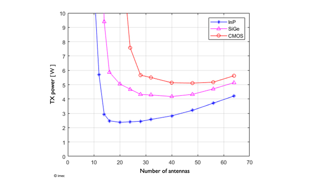
Figure 1 PA Tx power vs. number of antenna elements for a constant array EIRP, comparing InP, SiGe and CMOS PAs.
BRINGING InP TO MATURITY
Creating InP heterojunction bipolar transistors (HBTs) for 100 GHz and higher frequency systems requires, first, a mature and cost-efficient InP technology and, second, an approach to integrate InP and Si components into a complete system. To meet both challenges, heterogeneous integration of a III-V material such as InP with CMOS is key. CMOS will be the predominant technology used for calibration, control, beamforming and data conversion.
To meet the speed, efficiency and output power needed for these wireless systems, imec envisions InP HBTs fabricated on a 300 mm (12 in.) Si wafer platform. Today, compared to Si, InP wafers are small—under 6 in.—and devices are fabricated using serial processes such as e-beam for gate lithography, and the contact metallization is gold-based. InP is brittle, one of the most prominent challenges. None of these are compatible with CMOS fabrication.

Figure 2 Nano-ridges fabricated with InGaAs.
To use InP with Si, imec is researching ways to transfer III-V materials onto Si. Due to the large lattice mismatch between both materials, growing InP on Si usually introduces defects, mainly threading dislocations and planar. These induce leakage currents that can dramatically deteriorate device performance or impair reliability because the defects capture and release carriers at RF frequencies. To address the defects generated when directly growing InP on Si, imec is developing a fabrication process called nano-ridge engineering, which selectively grows the III-V material in pre-patterned structures or trenches in the Si (see Figure 2). These high aspect-ratio trenches are very effective, trapping the defects in the narrow bottom part and growing high-quality, low defect material out of the trench. At the same time, overgrowing the nano-ridge widens it near the top, forming a solid base for a device stack. Reducing the pitch between nano-ridges enables them to merge to create a local plate of III-V material.