
Recently, imec demonstrated box-shaped nano-ridges fabricated with 53 percent InGaAs, which efficiently trapped the threading dislocations in the trench. The nano-ridges were successfully grown both standalone and in a guided template. imec is using the same approach—combining InGaAs nano-ridge engineering with insights from earlier demonstrations of InGaP/GaAs nano-ridge HBTs—to develop a heterostructure stack for 140 GHz applications.
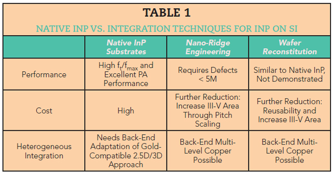
Other than direct growth such as nano-ridge engineering, InP can also be placed on Si using small InP substrates as the starting material. Called wafer reconstitution, high-quality InP substrates would be diced and sorted into non-patterned tiles during wafer fabrication, with the tiles subsequently attached to a Si wafer, planarized and processed in the fab. Table 1 assesses the performance, cost and heterogeneous integration potential of the direct growth and wafer reconstitution options compared to native InP substrates.
SYSTEM LEVEL CO-INTEGRATION
Obtaining a mature and cost-efficient InP technology through direct growth or wafer reconstitution is only part of the challenge, however. The resulting components need to be integrated into a complete system comprised of various building blocks in III-V and CMOS technologies, such as InP HBTs for PAs or CMOS for the beamforming transceiver. This poses a set of integration challenges. imec is looking into monolithic (2D) integration of III-V and Si devices in the same plane and 2.5D and 3D integration approaches for heterogeneous integration.
State-of-the-art PCB technology is continually being optimized to support higher frequencies, including reducing the pitch and optimizing materials and layout. 2.5D integration uses Si interposers—a chip or layer with lithography-defined connections and possibly through Si vias—to connect III-V and Si die. While this technology has been optimized for high speed digital applications (see Figure 3), it requires development to optimize it for RF. imec is evaluating dielectrics and various thicknesses of the metal layers to achieve low loss, high frequency interconnects. Options include high resistivity Si substrates or thick dielectric layers to distance the metal layers from the lossy substrate; also, a very thick redistribution layer, an extra metal layer to reduce metal loss. imec is also developing the capability to integrate high-quality passives for certain circuit applications.
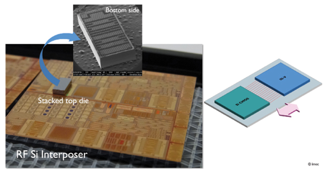
Figure 3 Top view of an RF interposer with a Si stacked top die.2
2.5D AND 3D: KEY FOR HETEROGENEOUS INTEGRATION
Why 3D integration? As frequency increases, wavelength decreases and the area of an antenna array shrinks accordingly. Above 100 GHz, the antenna pitch gets smaller than the front-end circuit pitch, as the area of mmWave RFICs hardly shrinks. So the footprint of the antenna array sets the size constraints; to fit everything underneath the antenna, heterogeneous integration using the third dimension becomes necessary.
Over the last decade, tremendous progress has been made with 3D interconnects, particularly reducing the interconnect pitch for wafer-level applications—i.e., wafer-to-wafer, die-to-wafer (see Figure 4).3 For wafer-to-wafer or hybrid bonding, imec has achieved pitches below 1 μm and can push this down to below 500 nm. The same trend to reduce the pitch holds for die-to-wafer bonding and die stacking using micro-bumps.
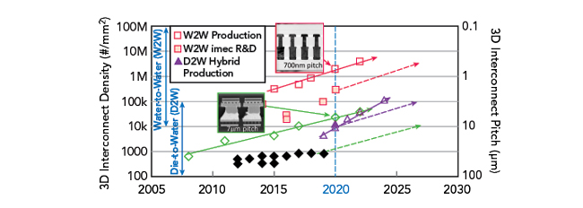
Figure 4 3D interconnect technology roadmap. Includes data from H.-S. Philip Wong, et al.4 and Techinsights.
Several challenges are shared between the two integration schemes for >100 GHz cases. First, they both rely on having a fine via or micro-bump pitch below 100 μm. Second, they must accommodate large numbers of connections for routing the RF, DC, IF and digital signals. Finally, both the trace and space dimensions need to be much smaller than 50 μm, preferably between 5 and 10 μm.
There are also differences between the two schemes (see Figure 5). In the case of 2D or 2.5D integration, the III-V device sits next to the CMOS IC, enabling better thermal management because both die can be in direct contact with a heat sink. The disadvantage is that the footprint may need to be extended in one dimension for some applications, meaning this architecture only enables 1D beam steering. In comparison, 3D integration enables all the die and circuits to fit under the antenna and enables 2D beam steering across a hemisphere. 2D beam steering is necessary for 5G and similar applications to minimize penetration losses and increase reach. With 3D, thermal management is more challenging and, of course, 3D integration is more complex, having unique processing challenges.
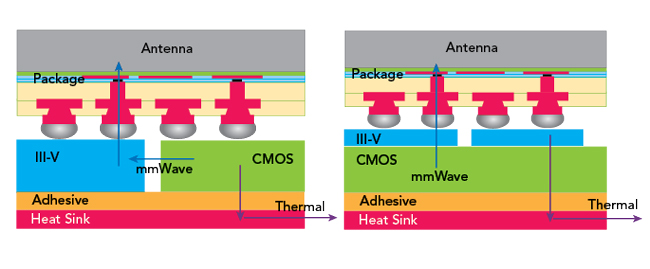
Figure 5 2/2.5D integration using a Si interposer to connect the III-V and Si die (a). 3D integration where the III-V die are stacked on the Si (b).
SYSTEM TECHNOLOGY CO-OPTIMIZATION
The choice of integration and packaging solutions ultimately depends on the application. Because so many options are available, imec has launched a system technology co-optimization (STCO) program to guide the technology choices at the system level. The STCO methodology uses architecture and application constraints, assessing signal loss, bandwidth, heat dissipation, mechanical stability and cost. Considering these parameters together enables trade studies to determine the appropriate technology and device designs for 6G.
References
- C. Desset et al., “InP/CMOS Co-integration for Energy Efficient sub-THz Communication Systems,” IEEE Global Communications Conference, December 2021.
- X. Sun et al., “Cost-Effective RF Interposer Platform on Low-Resistivity Si Enabling Heterogeneous Integration Opportunities for Beyond 5G,” IEEE 73rd Electronic Components and Technology Conference, June 2022.
- E. Beyne, “3D System Integration: Technology Landscape and Long-Term Roadmap,” Roadmap on 3D Interconnect Density Forum, International Solid-State Circuits Conference, February 2021.
- H.-S.P. Wong et al., “A Density Metric for Semiconductor Technology,” Proceedings of the IEEE, Vol. 108, No. 4.