
From these definitions we can conclude that the first two factors, FVmin and FGain, are limited by the device choice, while the last two factors, FMatching and FWaveform, are limited by design choices. Previous topologies aimed at improving the maximum efficiency of the PA were limited to only increasing FMatching and FWaveform through design choices.
CLASS B PA THEORETICAL EFFICIENCY REVIEW
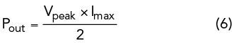
In Class B operation, the transistor is biased at the threshold voltage (VTH) and only conducts current during half of the cycle. When the device is on, the drain current is proportional to (Vin – VTH). Therefore, the drain current can be modeled as a half-wave rectified sine wave. Although the transistor drain current has large frequency content, the passive output network ensures that only the fundamental tone reaches the load. Using Fourier series analysis, we can define the maximum output power as:
The peak voltage swing at the load, Vpeak, can be described in terms of the supply voltage, VDD, and the knee voltage, Vknee, to include the effects of the device choice:
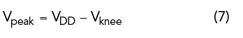
The DC power dissipation of the transistor can be expressed using the maximum current going through the load, Imax, as shown in the following equations:
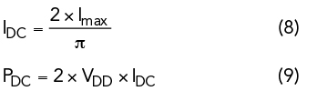
Finally, the maximum theoretical drain efficiency (DE) of an amplifier operating in Class B mode can be expressed by combining equations (6) through (9), as shown in equations (10) through (13).
Equation (13) shows the canonical Class B maximum efficiency of 78.5 percent when the Vknee is zero. In addition, Equation (13) also establishes the relationship between Vknee and the DE, ηclass-B, as previously shown using the proportionality constant FVmin in Equation (1).
DUAL-DRIVE PA
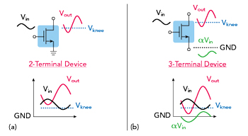
Figure 2 Conventional common source (a) and Dual-Drive (b) topologies, showing gate, drain and source waveforms.
The new patented Dual-Drive™ topology enables additional design freedom in improving PA performance by artificially reducing the knee voltage of the device, increasing the factor FVmin and in turn increasing the overall PAEmax of the PA. When a transistor is only driven at the gate, the device maximum efficiency is dictated by the device conduction angle and the knee voltage, Vknee. Vknee indicates the transition region between the linear and saturation region of a transistor and is a technology-specific physical parameter inherent to the physical device’s fabrication process and size. Moreover, Vknee reduces the output voltage and drastically impacts the achievable DE and overall efficiency of a PA.
In the Dual-Drive™ topology, Falcomm exploits the transistor as a three-terminal device and drives both the gate and the source terminals with out-of-phase inputs Vin and αVin (0<α<1), as shown in Figure 2. Assuming short terminations for all harmonics at the drain node, the source voltage now swings below ground while having an in-phase relationship with the drain voltage, increasing the maximum drain output voltage swing by αVin. This increased output voltage swing can be attained without increasing the supply voltage, which means that the maximum DE is increased in the Dual-Drive™ topology by a factor greater than 1.
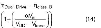
Falcomm demonstrated for the first time that through the Dual-Drive PA architecture they are able to artificially reduce/cancel out the knee voltage of the transistor, allowing for the maximum theoretical efficiency of a PA to be fundamentally increased beyond that of any PA class and topology as shown in Equation (14).
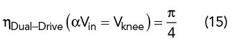
When the maximum voltage swing at the source is equal to the knee voltage of the transistor (αVin=Vknee), the theoretical maximum DE for the Dual-Drive PA will reach the maximum theoretical efficiency of the class B PA, π/4, as shown in Equation (15).
The strength of the source swing depends on α, which is a design constant that can be adjusted. Figure 3 shows that with varying α, there is a tuning tradeoff for PA designers to balance between power gain and the achievable efficiencies of the Dual-Drive PA transistor core. These results show that by employing the Dual-Drive architecture, the efficiency lost by the Vknee of the transistor can be recovered. In addition, Falcomm’s analysis of the Dual-Drive PA is consistent with Equation (1).
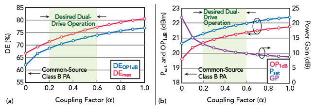
Figure 3 Large-signal load-pull simulations of low voltage CMOS transistor: DE (a) and Psat, OP1dB and power gain (b) vs. coupling factor.
BENEFITS OF THE DUAL-DRIVE PA
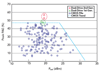
Figure 4 Dual-Drive PA Psat and PAE compared to CMOS PAs.
The benefits of the Dual-Drive PA topology are summarized as follows: first, increasing the source terminal coupling coefficient, α, can fundamentally increase the PA core DE beyond that of any other PA topology; second, higher DE can be maintained even at reduced supply voltages since the effect of Vknee under a lowered supply can be mitigated and third, the maximum output power can be increased while reducing the device modulation distortion, since the active device spends more time in its saturation region and less in triode.
Furthermore, the parallel input resistance of the transistor is reduced since the typically large device gate impedance is combined in parallel with its low device source impedance, aiding the design of broadband and low loss inter-stage matching networks without the need to implement lossy de-Qing resistors.
Finally, the Dual-Drive PA can mitigate the reliability issues of voltage peaking typically seen in complex harmonic-shaping PAs (Class J or continuous-mode Class F PAs). Therefore, the Dual-Drive PA is particularly suitable for high reliability space applications that mandate consistent operation in harsh environments while achieving ultra-high efficiency levels.
Initial efficiency measurement results from Falcomm’s first and second generation low-power CMOS Dual-Drive PA prototypes in comparison with state-of-the-art PAs at the same frequency band are shown in Figure 4. These initial results demonstrate that the Dual-Drive PAs are at least 25 percent more efficient than conventional PAs; which, based on estimates and discussions with one of Falcomm’s potential customers building micro-GEO satellites, could translate into $350,000 in launching cost savings per satellite.