
The first generation 30 GHz Dual-Drive™ power amplifier (PA) using a 45 nm silicon on insulator (SOI) process achieves 50 percent power-added efficiency (PAE) for a two-stage proof-of-concept, which is the highest efficiency ever achieved for a two-stage PA at 30 GHz on CMOS.
The world’s dependence on wireless communications is ever increasing within our daily lives, spanning multiple industries such as automotive, health care, consumer products, space communications and travel, scientific and military. Powering these new opportunities in wireless communications is the PA, which enables wireless transmission of data around the world.
With a compound annual growth rate of ~12 percent, the $16 billion PA market is one of the main driving forces enabling the advancement in wireless communication systems.1 Falcomm is working toward radically improving PA products for the wireless communications market.
Modern PAs are expected to support high-order modulation signals (e.g., 256-/1024-/4096-QAM) with OFDM, increasing peak-to-average power ratio (PAPR) specifications. Yet, these high PAPR levels can lead to less than desired average PAE at output back-off levels given current PA topologies. Therein lies the issue where the PA serves both as the enabler and the limiter for the desired implementation of advanced communication systems.
While the PA can service such high-order modulation schemes, it may inefficiently consume most of the power budget within a given wireless communication system, where most of the wasted energy is dissipated as heat. Given the ever increasing stringent communication protocols and requirements, high performance PAs are of paramount importance in the successful and rapid adoption of commercial next-generation communication networks.
Increasing the efficiency of PAs can greatly benefit the entire wireless communication market, which includes mobile devices, wearables, cellular base stations, cellphones, radar and other emerging markets.
For example, cost of ownership for cellular base stations is becoming a bigger concern for network operators as the deployment of 5G mmWave infrastructure takes place. In 2021, network operators spent about $120 billion for electricity in cellular base stations, where more than 50 percent of the energy consumption was from inefficient PAs. Therefore, increasing the efficiency of PAs will directly translate to reducing the electricity bill and carbon footprint of the wireless network infrastructure.
Another frontier for next-generation wireless communications systems is in space, where there is renewed interest and a desire to expand the robust low Earth orbital (LEO) economy and deploy a satellite infrastructure for reliable communication networks (such applications are Wi-Fi from space, cellular access to remote locations and intra-space communication, to name a few) and maintain a constant human presence in LEO to facilitate the next generation of space travel.
While commercial spacecraft manufacturers like SpaceX have helped reduce rocket/payload launch costs to less than $2,000 per kilogram,2 these costs still pose a high barrier to entry for companies with emerging new technologies, and they incur additional expenses to government agencies like NASA. Falcomm’s customer interactions with satellite manufacturers found that battery and solar cell loads account for a significant portion of a satellite’s weight. In some cases of Earth-to-space communication modules within satellites, the PA can be responsible for nearly 80 percent of the energy budget.
A more efficient PA can greatly ease thermal management requirements and reduce battery and solar cell sizes, but most importantly it can lower manufacturing and launch costs for satellites. For example, a micro-geostationary orbit (GEO) satellite manufacturer estimates that every 10 percent increase in PA efficiency will translate to $150,000 of launch cost savings per spacecraft due to the reduction in battery and solar cell weight. The estimated savings do not include the reduction in manufacturing and thermal management costs due to higher PA efficiency.
EXISTING PA TOPOLOGIES
The demand for more efficient and more linear PAs has driven extensive research to improve performance at the device level, for example increasing the fmax/ft of the transistor.3 In addition, improvements in the back end of the line processes such as thicker and lower-loss top metal layers have increased the performance of passive components, which has allowed a further increase in efficiency and output power.4
The increased fmax/ft metrics of the transistor device, however, do not necessarily lend themselves to improved PA performance, as, typically, the smaller lithography nodes have reduced voltage supply overhead and smaller breakdown limits, making apparent the tradeoff in device performance and reliability.
With regard to circuit topology improvements, to this date, almost all PA designs rely on common-source or common-gate topologies and are mainly focused on increasing peak/power-back-off (PBO), PAE and maximum output power (Pout) by presenting multi-harmonic terminations to the output of the PA, as accomplished in the Class F, Class J and their inverse and continuous-mode operations.5
A topology that has gained popularity in recent years is the harmonic-tuned PA and its different variations. This topology takes advantage of adding load terminations at the fundamental frequency and at some of the harmonics to increase the maximum PAE of the amplifier. Most modern technology nodes exhibit an fmax/ft between 100 and 300 GHz; therefore, at mmWave frequencies, the harmonic content might not be substantial enough to make a major improvement in efficiency. Additionally, passive networks that can provide harmonic tuning tend to be complex and lossy, further reducing the efficiency enhancement. Even though this technique shows low to moderate efficiency improvements, the beforementioned drawbacks hinder its adoption in commercial applications.
Recent efforts have also focused on further improving efficiency based on circuit topologies that can support complex modulation methods, such as stacked, outphasing, mixed-signal, reconfigurable and Doherty PAs.6,7 However, in modern Si processes with nanometer sized technology nodes that employ supply voltages of less than 1 V per stacked transistor (2 V for cascode devices), these reported techniques see diminishing returns on PAE and Pout since the transistor knee voltage, Vknee, becomes a significant portion of the supply voltage. Moreover, an extra reduction in supply voltage is often observed in practical deployment to ensure device reliability.
This is especially relevant for mmWave array operations, where array element couplings result in substantial antenna impedance mismatches (VSWR) and undesired large PA output voltage/current swings. Although the reported techniques have improved overall PA efficiency at mmWave frequencies, their operating principles are incapable of theoretically surpassing the linear mode operation PA core efficiency of the Class B common-source topology without resorting to lower conduction angles or harmonic shaping.
Beyond solid-state technology, traveling wave tube (TWT) amplifiers have been commonly used in satellite transceivers due to their high-power capabilities and high efficiencies (greater than 90 percent). However, TWT amplifiers are extremely bulky with form factors spanning several tens of centimeters and cannot support modern communication systems due to the reduced antenna size and spacing requirements of array-based architectures at higher frequencies (greater than 1 GHz).
Therefore, ultra-efficient high-power millimeter-sized solid-state PAs are critical for the successful and rapid adoption of next-generation communication networks since they are superior to other alternatives in transceiver power efficiency, thermal management requirements and overall communications channel performance.
EFFICIENCY CONSIDERATIONS FOR PAs
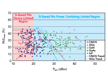
Figure 1 Published saturated output power vs. maximum PAE for 20 to 50 GHz PAs.
Figure 1 shows Psat versus PAEmax for previously published PAs ranging from 20 to 50 GHz.8 There is an inherent tradeoff between Psat and PAEmax. In addition, there exist two distinctive power/efficiency regions for PAs delimited by Psat. In the red region, called the device limited regime, efficiency is limited by the technology or device performance characteristics and to some extent by the design topology.
In the blue region, called the circuits/combiner limited regime, an increase in power is attained by employing different power combining techniques and, therefore, efficiency is limited by the losses of the output combiner network. This shows a clear tradeoff between saturated output power and maximum efficiency.
Moreover, when considering energy efficiency in PAs, PAE can be characterized by the four independent factors shown in the following equations:

where the first factor (FVmin) is associated with the maximum allowed output voltage swing, which is determined by the knee voltage of the device and the supply voltage; the second factor (FGain) is related to the gain of the device or the necessary driving power needed to saturate the PA; the third factor (FMatching) relates to the passive efficiency of the output network and the last factor (FWaveform) is a constant that depends on the PA gate biasing.