
DUAL-DRIVE PA SUPERIOR PERFORMANCE
The first technology demonstration was implemented using the GlobalFoundries 45 nm RFSOI. The chip occupies a total area of 1.3 × 1.2 mm2 with a core area of 0.25 mm2.9 Figures 5 and 6 summarize the Dual-Drive PA’s continuous wave performance with different supply voltages (1.7 and 1.9 V), achieving a maximum OP1dB of 19.1 dBm at 31 GHz with less than 1 dB variation from 23 to 34 GHz.
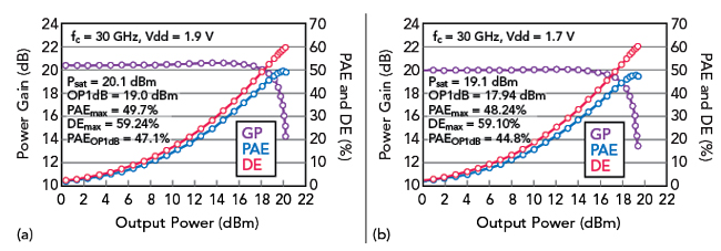
Figure 5 Measured power gain and efficiency vs. output power of the initial technology demonstration (version 0) of the Dual-Drive PA at 30 GHz, biased at 1.9 (a) and 1.7 (b) V.
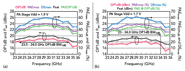
Figure 6 Large-signal CW measurements of the initial technology demonstration (version 0) of the Dual-Drive PA vs. frequency, biased at 1.9 (a) and 1.7 (b) V.

Figure 7 Measured single carrier, 64-QAM performance of the Dual-Drive PA, biased at 1.9 (a) and 1.7 (b) V.
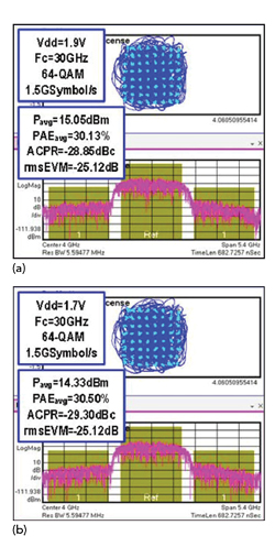
Figure 8 Measured single carrier, 64-QAM constellation and spectrum performance of the Dual-Drive PA, biased at 1.9 (a) and 1.7 (b) V.
The Dual-Drive PA achieves a maximum PAE of 50 percent and maximum DE of 60 percent at 29 GHz. This is the highest reported efficiency for a two-stage CMOS PA in this frequency range. Moreover, a PAE greater than 40 percent is maintained across the entire bandwidth from 24 to 35 GHz.
The efficiency results are met with great linearity performance as well. For example, OP1dB and Psat are within 1 dB of each other, which translates to a maximum PAE at OP1dB of 47.4 percent. Excellent linearity is demonstrated through extensive modulation measurements shown in Figures 7 and 8. For example, for a 9 Gb/s 64-QAM signal without digital predistortion (DPD), the Dual-Drive™ PA achieves an average Pout of 15.1 dBm and average PAE of 30.2 percent with a -25 dB rms error vector magnitude at 30 GHz. The efficiency performance is maintained at supply voltage levels that are 20 percent lower than the rated supply voltage, which positions the technology for high reliability applications.
The first generation 30 GHz Dual-Drive PA using a 45 nm SOI process achieves 50 percent PAE for the two-stage proof-of-concept, which is the highest efficiency ever achieved for a two-stage PA at 30 GHz on CMOS. Falcomm has been further developing and maturing the technology and newer tested prototypes are reaching even higher efficiencies with PAE reaching the 55 percent mark for a two-stage PA and average PAE of 34 percent using a 9 Gb/s 64-QAM signal at 30 GHz, which is a higher average efficiency than a Doherty PA can offer but with half the Si area.
CONCLUSION
Falcomm is focusing on developing its core technology into a product catalog with PAs of different power levels, frequency ranges, gain and packaging that will bring a better value to satellite, base stations and handheld device manufacturers. Falcomm believes these results demonstrate that its technology will become the industry standard for PAs and, based on current design efforts, is confident that it can push the technology further.
References
- “RF Power Amplifiers – Global Market Trajectories & Analytics,” Research and Markets, April 2021, Web: www.researchandmarkets.com/reports/5141446/rf-power-amplifiers-global-market-trajectory.
- I. Williams, “Boost-Phase Missile Defense Interrogating the Assumptions,” Center for Strategic and International Studies, June 2022, Web: www.csis.org/events/boost-phase-missile-defense-interrogating-assumptions.
- S. Lee, B. Jagannathan, S. Narasimha, A. Chou, N. Zamdmer, J. Johnson, R. Williams, L. Wagner and J. Kim, “Record RF Performance of 45-nm SOI CMOS Technology,” IEEE International Electron Devices Meeting, December 2007, pp. 255–258.
- O. Inac, M. Uzunkol and G. Rebeiz, “45-nm CMOS SOI Technology Characterization for Millimeter-Wave Applications,” IEEE Transactions on Microwave Theory and Techniques, Vol. 62, No. 6, June 2014, pp. 1301–1311.
- S. C. Cripps, P. J. Tasker, A. L. Clarke, J. Lees and J. Benedikt, “On the Continuity of High Efficiency Modes in Linear RF Power Amplifiers,” IEEE Microwave and Wireless Components Letters, Vol. 19, No. 10, October 2009, pp. 665–667.
- S. Hu, F. Wang and H. Wang, “A 28-/37-/39-GHz Linear Doherty Power Amplifier in Silicon for 5G Applications,” IEEE Journal of Solid-State Circuits, Vol. 54, No. 6, June 2019, pp. 1586–1599.
- E. F. Garay, D. J. Munzer and H. Wang, “26.3 A mm-Wave Power Amplifier for 5G Communication Using a Dual-Drive Topology Exhibiting a Maximum PAE of 50 Percent and Maximum DE of 60 Percent at 30 GHz,” IEEE International Solid-State Circuits Conference, February 2021, pp. 258–260.
- H. Wang, T. -Y. Huang, N. Sasikanth Mannem, J. Lee, E. Garay, D. Munzer, E. Liu, Y. Liu, B. Lin, M. Eleraky, H. Jalili, J. Park, S. Li, F. Wang, A. S. Ahmed, C. Snyder, S. Lee, H. T. Nguyen and M. E. D. Smith, “Power Amplifiers Performance 2000-Present,” Georgia Tech Electronics and Micro-System Lab (GEMS), August 2021, Web: https://gems.ece.gatech.edu/PA_survey.html.
- E. F. Garay, D. J. Munzer and H. Wang, “A 150 GHz Lens-Free Large FoV Regenerative 2 × 2 Transceiver Array With 31 Percent DC-to-EIRP Efficiency and −70 dBm Sensitivity for a 70 cm Bidirectional Peer-to-Peer Link,” IEEE Journal of Solid-State Circuits, Vol. 57, No. 7, July 2022, pp. 2102–2113.