
Recent advances in silicon technology have aggregated many essential functions required by electronic warfare (EW) systems within a single device. These highly integrated components not only simplify traditional EW design architectures, but also improve critical performance metrics. Because of reduced size, weight and power (SWaP) and cost, they also open new markets and applications that were previously impractical. In addition, emerging standards for embedded systems offer opportunities to harness these benefits.
Presented with diverse challenging requirements and tight schedules, EW system designers must take advantage of any new suitable resources, design strategies and standards to meet these increasingly difficult goals. This article discusses how these advantages can advance the capabilities of new EW platforms.
THREE CLASSES OF EW
The overarching mission of EW is the exploitation of any part of the electromagnetic spectrum to achieve superiority over the adversary, across virtually every deployed military platform in every warfighting arena, including land, sea, underwater, air and space. The hallmark of EW is the never-ending escalation of techniques and capabilities to gain an advantage over the opponent—before they counter the challenge with a new design.
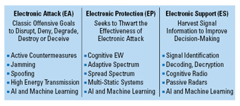
Figure 1 While the three generic classes of EW systems require diverse capabilities, they share underlying technologies.
EW is roughly divided into the three major classes (see Figure 1). Electronic attack (EA) promotes offensive objectives to disrupt, deny, degrade, destroy or deceive, while electronic protection (EP) offers defensive tactics to thwart the effectiveness of EA. Electronic support (ES) exploits signal information to extract actionable intelligence of all types to improve both strategic and tactical decision-making. Although these three classes have different objectives, they all benefit from improvements in digital signal processing, so effective new technology deployed in one class is often quickly adopted by the others.
OPERATIONAL REQUIREMENTS
Modern EW systems are shifting away from older dish antennas, which are large, heavy and cumbersome to rotate and elevate to aim the transmit/receive beam pattern in a particular direction. Instead, phased array antennas now offer many significant advantages for virtually all platforms. They consist of a linear or two-dimensional planar array of antenna elements. By adjusting the relative phase of each element’s signal, the beam pattern can be electronically steered to any angle—virtually instantaneously—without having to mechanically turn the array. When installed on the surface of an aircraft or the belly of an unmanned vehicle, a phased array antenna can quickly adapt to threats and track multiple targets without the bulky mechanical structures required for a dish. Although ideally suited for airborne and unmanned aerial vehicle radars, where size is critical, larger phased arrays are extremely effective for precision ground and maritime radars, especially for fire control and countermeasure systems.
Phased array systems require extensive digital signal processing (DSP) resources to acquire and generate the signals for each of the many elements, precisely control the relative phase shifts between the elements and implement beamforming algorithms. This poses several challenges for the traditional EW system architecture, where the antenna array is mounted in a location best suited to capture signals—perhaps on an antenna mast—and connected to an equipment bay through dozens of long RF cables for the many elements. To ensure beam steering integrity, accurate and stable phase matching between the cables is essential, despite temperature fluctuations, cable movement, aging and maintenance. Adding to the challenges, analog signals flowing from remote antennas or sensors suffer signal degradation from cable losses and susceptibility to interference from powerful antenna transmitters, inter-channel crosstalk and power generation equipment.
Signal latency is often critical to many EA and EP systems dedicated to fire control and countermeasures. Here, a signal is received, a counter response signal is computed and transmitted, all with minimum overall delay. This latency often defines the limiting performance of such systems. Unfortunately, the latest analog-to-digital converters (ADCs) and digital-to-analog converters (DACs) with the highest sampling rates favor gigabit serial JESD204 interfaces. Even though they achieve high instantaneous bandwidth, the serial interfaces on these devices rule out their use in low latency EW applications.
New EW techniques often require significant increases in RF signal complexity to confront and overcome the latest threats and to further exploit targets. Here, sophisticated radar pulse waveforms are developed to extract more information from targets in the presence of noise, jamming and other countermeasures. Signals are now more heavily encrypted for enhanced security against interception and eavesdropping. For low latency EA and EP systems, this means more real-time DSP to maintain computational throughput for an appropriate counter response with minimal delay. This is usually accomplished with FPGAs, although some of the higher complexity tasks can require GPUs or artificial intelligent (AI) engines.
Finally, phased array systems magnify the data converter and signal processing issues described because each of the numerous elements now requires its own dedicated ADC, DAC and DSP functions. All the requirements and challenges above will only grow as EW systems evolve, so it is imperative to identify and exploit new technologies, architectures and techniques to maintain competitive advantage.
BENEFITS OF NEW SILICON
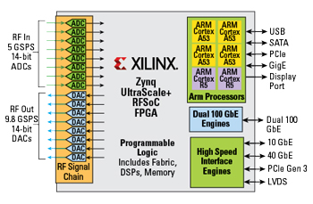
Figure 2 The AMD Xilinx RFSoC has the essential signal processing elements needed for EW systems.
Fortunately, Xilinx offers two advanced FPGA families that combine several of the critical EW functions defined above within a single device. The first is the highly popular RF system-on-chip (RFSoC) that went into production in 2018. The RFSoC is part of the Xilinx UltraScale+ FPGA Zynq architecture based on a 14 nm silicon geometry (see Figure 2). Now in the Gen3 revision, it includes eight 14-bit ADCs sampling at 5 GSPS to support direct RF digitization of input signal frequencies up to 6 GHz, and eight 14-bit DACs sampling at 9.8 GSPS.
Each ADC is equipped with direct digital down-converters with programmable frequency tuning and decimations of ×1, ×2, ×4 and ×8. An additional decimation stage of ×16 is implemented in the FPGA, providing a maximum overall decimation of ×128 for narrower signal bandwidths. The DACs are equipped with matching digital up-converters with interpolation settings of ×1, ×2, ×4 and ×8. These two 8-channel RF data converters are connected directly to the Zynq FPGA fabric, eliminating the power, connections, complexity and latencies of the traditional interfaces to external discrete data converters.
An onboard, multicore ARM processor serves as a system controller, providing control, status, I/O and a 1 GbE interface to an external host. Two 100 GbE interfaces connect the RFSoC FPGA fabric to external devices at data transfer rates up to 24 Gbps in both directions.
Originally developed for the massive MIMO antenna requirements of 5G wireless, the RFSoC supports the key functions for eight elements of a phased array, including direct transmit/receive RF conversion, real-time DSP and control. By effectively addressing so many vital requirements, this new FPGA architecture was immediately attractive to EW designers. Its small size shrinks SWaP and cost, especially critical for air vehicles and small EW countermeasure systems, and it enables new system architectures providing significant performance enhancements.
This technology enables compact, small form factor (SFF) enclosures integrated within or behind the antenna array to hold the RFSoC devices and the RF circuitry for converting RFSoC L-Band signals to and from higher frequency antenna signals. Inside the RFSoC, digitized samples from the data converters connect directly to the FPGA fabric, drastically reducing latency compared to external discrete devices with serial JESD204 interfaces. DSP functions within the FPGA can locally apply the required phase shifts to the elements for beam steering receive and transmit signals and handling signal acquisition, triggering, waveform generation, time stamping and digital up- and down-conversion. These real-time front-end operations significantly offload back-end processing tasks.
Sensitive RF circuitry and data converters are now inside the SFF enclosure, eliminating the need for long analog RF cables with their many disadvantages. Instead, digitized payload signals are connected to the host system using gigabit serial links, a popular trend for embedded system interconnections. The RFSoC supports this architecture by providing two 100 GbE interface engines, each with four, full-duplex 25 Gbaud lanes. By equipping each subsystem with optical transceivers, multi-mode fiber-optical cables can deliver data at 24 Gbps across distances up to 100 m. These links are not only lighter, smaller and less expensive than RF cables, they are impervious to electromagnetic interference and maintain full signal integrity.
Because the RFSoC is a complete software radio subsystem on a chip, it opens many EW uses impractical with earlier technology. These include stand-alone SFF systems (see Figure 3) for monitoring stations, troop protection, agile countermeasures, fire control systems and smart munitions.
SOSA™ AND EW
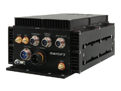
Figure 3 A ruggedized RFSoC enclosure for mounting directly behind a phased array EW antenna delivers digitized signals across dual 100 GbE optical interfaces using the VITA-49 data protocol.
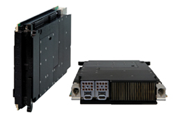
Figure 4 An RFSoC SOSA aligned 3U OpenVPX plug-in card has 20 VITA 67.3 backplane RF coaxial connectors and two 100 GbE optical I/O ferrules.
The Open Group Sensor Open Systems Architecture (SOSA™) Consortium released its long-awaited SOSA Technical Standard 1.0 in September 2021, defining the SOSA Reference Architecture. To comply with the Department of Defense (DoD) mandate for use of open systems architecture, its rules describe a limited set of well-defined open standard designs to be used in embedded defense systems. Drawing heavily on VITA standards, including OpenVPX, SOSA’s benefits include easier insertion of new technology, faster reaction to new defense threats and requirements, improved interoperability across vendors, longer lifecycle and lower cost for acquisition and maintenance.
With so many existing EW platforms in need of upgrades and a growing need for new, more capable EW systems, adopting SOSA is an obvious solution. SOSA specifies a subset of OpenVPX slots and module profiles for both 3U and 6U VPX, defining backplane pins for data, control and expansion planes to promote vendor interoperability. Most traffic flows across these planes use Gigabit Ethernet at rates of 1, 10, 40 and 100 Gbps, all popular standards widely used in commercial enterprise markets.
Another significant SOSA requirement is that all analog and digital I/O must flow through backplane connectors instead of the front panel, intended to simplify maintenance and improve reliability. This has a major impact on EW because of the high number of antenna signals required for phased array designs. Foreseeing this dilemma, engineers in VITA developed some remarkable new backplane connectors to handle devices like the RFSoC on SOSA plug-in cards with eight analog inputs, eight analog outputs and four clock and timing signals.
Now adopted by SOSA, these backplane connectors support products like the Mercury 5553 SOSA aligned RFSoC processor (see Figure 4). The unit has no front panel connectors (left) and two VITA 67.3 metal blind-mate backplane housings are visible in the rear (right). Each housing includes 10 coaxial nano-RF connectors rated for 20 GHz signal bandwidth, which support all the analog I/O signals from the RFSoC. Each housing has a 24-lane optical fiber ferrule supporting the two 100 GbE ports of the RFSoC.
NEW PROCESSOR AIDS EW
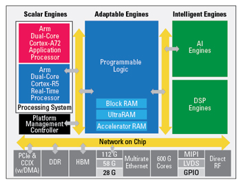
Figure 5 AMD Xilinx Versal AI Core ACAP heterogeneous processor integrates adaptable FPGA, DSP, AI engines, multicore ARM processors, network-on-chip, multi-rate Ethernet I/O and other system interfaces. Source: Xilinx
Xilinx’s latest Versal Adaptive Compute Acceleration Platform (ACAP) family adds capabilities for EW systems. The members of the family provide different blends of three processing resources: scalar processors (ARM CPUs), adaptable logic (FPGAs) and vector processors (GPUs and DSPs), as shown in Figure 5. Following the RF integration inspired by the success of the RFSoC, an upcoming version of ACAP will offer onboard direct sampling RF ADCs and DACs.
Of the many requirements for the EW classes shown in Figure 1, AI and machine learning (ML) will be used by all three: EA, EP and ES. AI capabilities such as inference, image processing, pattern recognition and signature detection are appropriate for EW and many other defense applications. ML is a subset of AI that can help automate and improve decision-making by assisting or replacing human operators, resulting in faster and more accurate responses.
The heterogeneous mix of ACAP resources enables designers to assign a task to the most suitable processing engine and adaptively reassign the resources as required. This flexibility of ACAP delivers up to 10x the performance compared to dedicated processors. Onboard, flexible high bandwidth memory (HBM) boosts the processing bandwidth for all the engines. To interconnect all these resources, ACAP includes an extremely wideband, configurable network-on-chip with a uniform interface and protocol to simplify system integration.
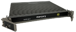
Figure 6 SOSA aligned 6U OpenVPX conduction-cooled plug-in card with two ACAP Versal AI devices with heterogeneous scalar, vector and logic processing for AI, DSP and ML EW applications.
Versal development tools support high-level design entry from frameworks, models, C-language and RTL coding. Users can create a custom development environment to suit project needs and programming preferences. Other Versal hardware/software platforms will evolve to speed EW development and support high-complexity and extreme performance requirements.
The flexibility of ACAP aligns with SOSA’s objectives for reusability and adaptability to new threats. As an example, the Mercury SCFE6931 (see Figure 6), is a 6U VPX SOSA aligned processor plug-in card containing two ACAP Versal AI Core Xilinx VC1902 devices.
SUMMARY
Since EW is an increasingly significant cornerstone of all defense organizations, the rapid adoption of new technologies and standards is imperative. Integrating data converters, FPGA resources and processors into a single RFSoC affords major benefits to performance while reducing SWaP and cost. Creating a heterogeneous mix of specialized processing resources afforded by the ACAP device enables a single, flexible platform to support a wide range of advanced AI and ML applications and deployment scenarios.
By adopting the newly released SOSA Technical Standard 1.0, system designers can comply with the DoD’s open systems architecture mandates to lower acquisition costs and extend system lifecycle. Harnessing these new complex technologies requires development tools that support high-level design entry and the flexible migration of tasks across many resources. Expect ongoing development of these tools and other new technologies to meet the constantly evolving EW needs of the warfighter.