
The CMC-SOIC8 ceramic SOIC8 surface-mount package is ideal for packaging RF/microwave MMIC and discrete devices for applications from DC to 18 GHz. This new addition to CMC's standard product line is fabricated using aluminum nitride (AlN), a ceramic material with thermal conductivity of 180 W/m-K, about 10 times higher than alumina. Because this package utilizes robust ceramic construction, it is highly reliable and temperature stable.
This article's primary focus is RF properties for the new CMC-SOIC8. This includes RF test, RF performance data and a description of a four coupled-line RF model that closely describes package performance. In addition, the fabrication method used to manufacture this package, advantages of cofired AlN when compared to other ceramic systems and key applications for the CMC-SOIC8 package are also discussed.
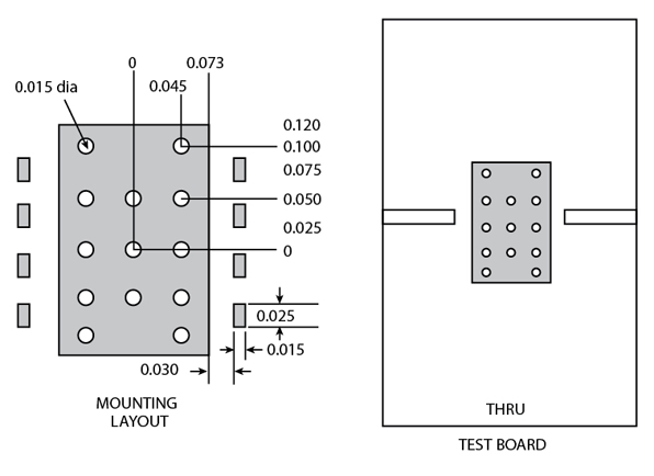
RF Test Mounting Configuration
The CMC-SOIC8 package has been characterized in a microwave test fixture using the mounting configuration and test board layout shown in Figure 1 . This configuration was chosen to be compatible with anticipated user topologies, namely microstrip transmission lines and via hole grounding. The material chosen for characterization to 20 GHz was Rogers 3003, 10 mil dielectric thickness and 1/2 oz copper, yielding a 50  line width of 24 mils. This line width minimizes any impedance discontinuity to the 25 mil wide pad of the package.
RF Measurements
Two port S-parameters were measured in a thru configuration using an HP8510B network analyzer. This configuration consisted of the CMC-SOIC8 reflow soldered to the test board shown. Internal to the package, a 50 alumina line (slabline) is brazed to the via grounded pad and ribbon bonded to opposing I/O lines, as shown in Figure 2 . The test fixture consisted of two precision 2.92 mm coaxial connector-to-microstrip launchers and a center block. The test board connects only one thru path because multiple connections to the CMC-SOIC8 package are electrically coupled and can significantly perturb a basic thru measurement.

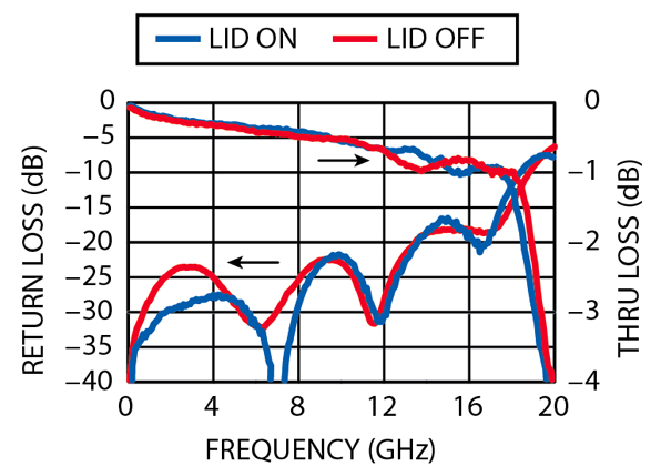
The measurement results, including fixture and PCB losses, are shown in Figure 3 for the two cases of lid on and lid off. Note that the cover, which is made of 96 percent Al2O3, has only a small affect on either parameter, especially since there was only a 5 to 7 mil space between the top of the slabline and the inside of the lid.
Package Model
When measuring the thru response touching the adjacent CMC-SOIC8 package lines produced a shift in the apparent resonance at about 20 GHz. Furthermore, when one of the adjacent lines was shorted to the topside ground a clear resonance occurred at approximately 10 GHz, which will happen for a quarter-wavelength coupled line shorted at one end and open at the other. These observations suggest that a coupled-line model is very important for this type of package since it will accurately predict a user's response for various adjacent line terminations.
The model shown in Figure 4 , developed and verified using the Microwave Office circuit simulator, consists of four coupled lines, each with gap coupling to ground, for the four I/Os on one side of the CMC-SOIC8 package. For the opposite side of the package the same model is used, observing the user and chip interface orientation for the port connections. The circuit uses physical transmission line models with an associated substrate definition (AlN, for example). The dimensions used correlate closely to the actual feature dimensions of the metal patterns. The coupled lines are broken into three sections to approximate the different gaps between lines along their length and the gap model approximates the capacitive coupling to ground at the ends of lines. This is a basic microstrip model and must be considered "first order." It does not solve for the actual fields of a wrap around conductor, for instance, and there are other approximations, but it predicts the dominant effects of line impedance and coupling to chip and user circuit connections. Due to its simplicity it is efficient and does not add excessive simulation time when integrated into larger circuits.
Figure 5 shows a response comparison between a measured and modeled CMC-SOIC8 package with thru line. In this case, for comparison, the slabline and test board lines were also part of the model. The modeled response has a sharper (higher Q) resonance than the real response and it is believed that, at resonance, the part is radiating energy, which is unaccounted for in the model (and very difficult to do). Additional discussion of RF performance is detailed in an application note available on the CMC Web site. The AWR model given can also be downloaded.

Co-fired Aluminum Nitride Package Fabrication
The CMC-SOIC8 package is fabricated using a proprietary process that combines high thermal performance AlN with internal and external metallization features constructed from tungsten metal. AlN is chosen for this application because it is an electrical insulator, but also an excellent heat conductor. Tungsten is chosen because it has a close thermal expansion match to AlN making the entire system dimensionally stable and resistant to thermal excursion induced stress. Also, it is a good electrical conductor and tungsten has a high enough melting temperature to make it compatible with the "co-fire" process.
The package fabrication process involves three distinct steps: the ceramic "green-fab" operation, where ceramic and metal powders are formed in the same geometry as the final package; the "firing" step, where this "green-fab" body is consolidated at a very high temperature to produce a fully dense ceramic substrate with both internal and external metallization; and a final finishing step, where the dense ceramic body is plated.
Advantages of Utilizing Co-fired Aluminum Nitride
The co-fired AlN process yields a number of critical advantages when compared to other ceramic approaches. Co-firing allows the incorporation of metal features, such as dense hermetic vias, within the ceramic body. This is a distinct advantage when compared to post-fire processes like laser drilling because:
- The final body is much stronger (drilled holes tend to be stress concentrators which initiate cracking)
- The process is less expensive (punching a green tape is much faster and less expensive than laser drilling, which is slow and results in a via with inconsistent surface chemistry)
- The resultant metallization layers and vias are hermetic
- The resultant metallization layers and vias are extremely uniform (plated metal thicknesses in laser drilled vias tend to be very non-uniform).
Aluminum nitride as a ceramic material provides a critical advantage when compared to other co-fire systems such as alumina or LTCC, because of AlN's excellent thermal conductivity: nine to 10 times greater than alumina and 90 times greater than LTCC. AlN is also an extremely strong ceramic material, particularly when co-fired with tungsten (which forms a metal re-enforced ceramic composite).
DC to 18 GHz Surface-mount Package Applications

Ideal market opportunities DC to 18 GHz for semiconductor and hybrid product in CMC-SOIC8 high thermal conductivity surface-mount package include:
- Gain and power stages for cellular base station, WCS, MMDS, WLL, 5.8 GHz bridge, C/X/Ku-band VSAT, digital Pt-to-Pt radios and test equipment
- Interposers to mount individual wire-bondable chips into a PCB-based multi-chip module or softboard assembly
- Amplifiers for fiber optics applications (OC48 and 192)
- VCOs
- Sampling phase detectors
- Detectors and limiters
- Broadband applications (2 to 18 GHz, 2 to 8 GHz and 6 to 18 GHz)
- Power supply and power control semiconductors (for example, semiconductors for power distribution and power supplies).
The aforementioned applications are ideal for the CMC-SOIC8 ceramic package due to its outstanding DC to 18 GHz performance, its excellent thermal conductivity as well as its inherent reliability and stability. CMC also offers semi-custom and custom SOIC package designs to meet application-specific mechanical and electrical requirements.
CMC Wireless Components, Phoenix, AZ (480) 496-5000. Circle No. 302