

Industry trends toward higher frequencies and more complex integrated systems require new design techniques and more extensive simulation.
Can you remember a time when RF standards drove such a rapid rate of change? In transitioning from 4G to 5G, frequencies have increased 40x—700 to 2600 MHz and 28 to 40 GHz—while automotive radar frequency bands have increased from 24 to 77 GHz. As frequencies increase, the density and complexity of system integration also increase, specifically with the integration of phased array antennas.
Trends toward higher frequencies have significant consequences for RF and microwave component and system design. Existing design flows require new techniques to keep pace with the design challenges in the 5G, automotive radar and aerospace/defense markets. Three of the top electronic design automation (EDA) challenges for designers of RF and microwave circuits, modules and systems are:
- Multilayer, multi-technology integration
- Electromagnetic (EM) effects on circuit simulation
- EM effects on system simulation.
MULTILAYER, MULTI-TECHNOLOGY INTEGRATION
Increasing RF frequencies, RF coupling and integration densities create challenges for designers. They must correctly lay out 3D avoidance-route, multi-technology RF modules to connect RFICs, MMICs, wafer-level packages, laminates, antennas and PCBs.
In a typical multi-technology scenario, chips from one technology mount onto different technology modules. Each technology has a substrate with layers, material properties, layout units and database resolution. There must be a mapping between the elements of the different substrates when placing a chip on the top-level module design; then, the layout tool must compute the proper 3D position of objects in the multi-technology design for 3D visualization and EM simulation. A good layout tool can work for both package and IC designs, and an efficient layout environment ultimately facilitates easier assembly of technologies, regardless of the design origin.
One approach EDA software takes is to provide intelligent mounting techniques that adapt when assembling different technologies and integrating databases. Intelligent mounting merges layers at the technology interfaces, such as a MMIC on a package that uses other technology databases. The IC substrate has a ground layer at the bottom, and that is an interface. When the IC mounts onto a package using intelligent mounting, the bottom interface of the IC maps to the top layer of the package, ensuring that the chip has the proper offset. The MMIC must then include design rule checks and layout versus schematic validation at the module level, not just the device, IC and board levels. These processes ensure error-free integration of multi-technology modules for manufacturing sign-off.
EM EFFECTS ON CIRCUIT SIMULATION
In a traditional RFIC design, EM simulators perform simulations for on-chip frequency-sensitive components, such as inductors and capacitors. Complicating the simulation is the modification of the original IC layout to extract and export the components to the EM simulator for analysis. Before the EM analysis can begin, the ports, material properties and simulation parameters must be properly set up. After simulation, multiport S-parameter results must be manually reconnected to simulate the active circuitry. Manual reconnection is error-prone and risks corrupting the design database.
Integration densities and layout infill requirements introduce increased RF coupling effects and longer simulation processes. To reduce simulation time and effort, the leading RF EDA software suites use a technique called EM and circuit “co-simulation.” With co-simulation, circuit designers do not need specialists to set up EM tools since correct port types are automatically assigned. Circuit simulations and EM interactions unite in one integrated workflow. Circuit designers can interactively include the 3D EM effects of packaging and interconnects during design exploration, tuning and optimization—not just for final verification of the completed design.
Other new approaches provide circuit designers with the ability to electromagnetically evaluate any portion of their RFIC, MMIC, RF module and RF PCB design without layout modifications using component and net extraction techniques, cutting EM simulation time. Mesh domain optimization can also provide orders-of-magnitude faster simulations of selected (extracted) components and nets.
EM EFFECTS ON SYSTEMS SIMULATION
Most experienced RF designers have endured the challenge of hand modifications to their carefully designed hardware to address cavity resonances and isolation issues. Those modifications can lead to intricate adjustments to multilayer PCBs and mechanics. Early simulation is the way to avoid this rework.
System architects must specify chipset designs to their circuit-level teams to ensure their system specifications are partitioned correctly to the RFIC designers. Modern EDA software suites can verify system performance with circuit-level accuracy by bringing models directly from circuit to system design tools, connecting circuit and system design teams and removing any source of error with a single model format. This workflow step can predict interference and coupling issues through integrated EM analysis, predicting high frequency layout effects on RF system performance. It also gives system designers a powerful troubleshooting tool to pinpoint board and module source coupling before building hardware prototypes.
KEYSIGHT EXAMPLE
Achieving first-pass success in simulation starts with a comprehensive strategy for circuit and system design. There are many steps in the RF workflow. Minimizing the number of imports and exports during design and simulation can save substantial time and reduce the chance of human input and export errors. Figure 1 illustrates an integrated workflow using Keysight PathWave EDA.
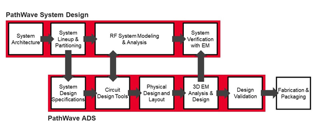
Figure 1 Keysight PathWave RF EDA workflow.
The OpenAccess coalition defines a set of application programming interfaces (APIs) and data formats that facilitate the interoperability of EDA software solutions. Keysight PathWave ADS and PathWave System Design are based on the OpenAccess database architecture and provide efficient assembly and routing of 3D, integrated RF module structures consisting of
- RFIC and chip-scale antenna layouts based on OpenAccess; for example, Virtuoso and EMPro
- PCB and laminate layouts based on ODB++; for example, Allegro, Expedition and Zuken
- ADS native MMIC and RF layouts.
PathWave ADS enables error-free assembly and 3D avoidance routing to interconnect RFICs, MMICs, laminates, wafer-level packaging, antennas and PCBs into multi-technology RF modules. It is important to be able to assemble multiple adjacent designs, implemented in different technologies, into a single workspace. Keysight's approach to intelligent mounting, called SmartMount, enables drag-and-drop, error-free assembly of mixed-technology components into a “simulate-able” 3D structure by automatically taking care of layer stack-up definitions, units and orientation (see Figure 2).
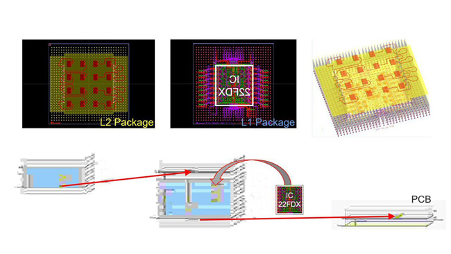
Figure 2 Intelligent mounting approach with ADS SmartMount. Credits: Design from Global Foundries and Fraunhofer IIS/EAS/IZM.
A multifunctional approach to building and assembling packages makes it straightforward for IC designers to account for package effects on IC performance. For example, after assembly, the ADS suite behaves as both a physical IC layout and package design tool, enabling hierarchical substructures as an IC tool and avoidance-route 3D interconnects as a package tool.
For circuit design, 3D EM circuit co-simulation enables RF circuit designers to electromagnetically analyze any portion of a design interactively without layout cookie-cutting and tedious port setup, ground references and 3D EM simulation parameters. Since the layout does not need modifications for EM simulation, the integrity of the original design is preserved. The introduction of manual modification errors, inherent in other 3D EM simulators, is avoided. Figure 3 illustrates 3D EM circuit co-simulation via RFPro in ADS.
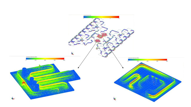
Figure 3 RFPro in the PathWave Advanced Design System.
The 3D EM results automatically combine with circuit simulation to analyze the EM effects on circuit performance from packaging, interconnect and coupling. This automation frees the RF circuit designer to do 3D EM analysis and EM circuit co-simulation spontaneously, without manual setup errors. The result is significantly faster EM circuit co-simulation setup—from weeks and months to just seconds and minutes.
A system-level path in the EDA workflow enables advanced virtual prototyping and design for RF system architects, array antenna designers, RF module designers, DSP engineers and system test engineers. The PathWave System Design tool enables RF designers to bring full EM simulated layout effects from their designs or prototypes into the EDA workflow to analyze leakage effects at the system level and pinpoint how to reduce layout risks before committing to hardware.
PathWave RFPro and System Design work collaboratively to perform an EM extraction and map values to the S-parameter file. Once mapped, all nodes versus all nodes can be accurately simulated, including cavity resonance effects caused by the enclosure. With this approach, designers can make precise fixes by visualizing the leakage effects in table form, with node versus node leakage ordered by severity.
SUMMARY
5G and next-generation radar systems use mmWave frequencies with complex modulation and have higher board layer density that push the limits of EM and circuit simulation, system simulation and packaging assemblies. RF system design challenges include multiple antennas, complex modulation, beam steering and sophisticated algorithms.
Keysight's PathWave Design software suite features 3D layout and assembly of multi-technology RF modules, including RFIC, MMIC and PCB. The 3D layout and assembly, together with interactive EM circuit and system analysis, accurately account for EM packaging effects during design. This workflow is an example of how EDA technology is evolving to improve the predictability of the RF design process and reduce design cycles.