
A miniaturized microstrip ultra-wideband (UWB) bandpass filter with dual notched bands and improved out-of-band rejection uses a modified square ring multi-mode resonator (MSRMMR). Four high-low impedance resonant cells are placed in the inner area of a conventional square ring multi-mode resonator (MMR), forming an MSRMMR to achieve harmonic suppression and size reduction. An E-shaped resonator is coupled to the MSRMMR to achieve dual notched bands.
UWB radio technology has become more popular for high speed wireless connectivity since the Federal Communications Commission’s decision to permit unlicensed operation in the band from 3.1 to 10.6 GHz in February 2002.1 UWB radio offers several advantages, such as higher data rate, lower transmit power and simplified error control coding. The UWB bandpass filter, one of the essential components of an UWB system, has received much attention in recent years. Several different designs have been proposed.2-6 Gomez-Garcia et al.2 directly cascaded highpass and lowpass filters, but insertion loss and overall circuit size were inevitably increased. A multilayer broadside-coupled structure has been used,3,4 but the multilayer structure is not compatible with existing microwave integrated circuit design. Song et al.5 used an MMR, but the filter had a narrow upper stopband. Wei et al.6 used a three-line coupled resonator, but selectivity was not ideal. Additionally, signals from existing wireless networks such as 5.8 GHz WLAN and some 8.0 GHz satellite communication systems can interfere with UWB transmissions. To address this, UWB BPF designs with notched rejection bands are emerging.7
Based on our previous work,8 we introduce a new miniaturized microstrip UWB bandpass filter with dual notched bands and improved out-of-band rejection using a MSRMMR. Four high-low impedance resonant cells are periodically placed within the inner area of a conventional square ring MMR. This achieves harmonic suppression and size reduction. Coupling an E-shaped resonator to the MSRMMR creates dual notched bands.
FILTER DESIGN
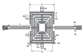
Figure 1 Layout of the UWB bandpass filter.
Four high-low impedance resonant cells are placed inside the free area of the conventional square ring MMR (see Figure 1). Each unit cell comprises two high impedance and two low impedance lines, cascaded alternately. The high impedance lines are loaded only at the sites connected to the ring, creating lumped form inductances, which do not influence the per unit length inductance of the main transmission lines. The low impedance lines are loaded in parallel with the main transmission lines, which adds distributed capacitance and increases the per unit length capacitance of the main transmission lines. This type of slow-wave loading mainly increases shunt capacitance in the UWB bandpass filter.
The effective characteristic impedance Z and propagation constant β are given by:


where L0 and C0 are the distributed inductance and capacitance without loading per unit length, respectively; C1 is the effective distributed capacitance caused by the periodic loading per unit length. Equation 2 shows the propagation constant is increased by the periodic capacitive loading. An increased propagation constant means a shorter physical structure can be used to yield the required electrical length compared to a conventional transmission line. The slow-wave loading does not increase the circuit area, as it is placed within the outer square ring.9 Therefore, a compact UWB bandpass filter with improved out-of-band rejection and good selectivity can be achieved using this slow-wave structure.
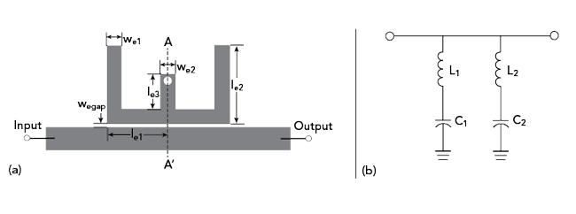
Figure 2 Layout (a) and equivalent circuit (b) of the coupled E-shaped resonator.
FILTER DESIGN WITH NOTCHED BANDS
To realize band-notched characteristics, an E-shaped resonator is added to the basic UWB bandpass filter. This structure is simple and flexible, consisting of a stepped impedance hairpin resonator centrally loaded with a shorted stub. Figure 2 shows the layout of the resonator coupled to a section of the main transmission line and its equivalent circuit. Its resonant properties can be determined by even-odd mode analysis. Under excitation, the resonator’s electric field (E-field) exhibits either an even or an odd mode distribution property (see Figure 3). For the odd mode, the E-fields are anti-symmetric, distributed along the A-A' axis, and there is no E-field on the shorted stub, as shown in Figure 3a. For the even mode, the E-fields exhibit a symmetric distribution along the A-A' axis on both the open and shorted stub, shown in Figure 3b.
The even-odd mode resonant frequencies can be expressed as

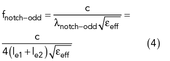
where λnotch is the wavelength of the center frequency of the notched band, ƒnotch is the center frequency of the notched band, εeff is the effective dielectric constant and c is the speed of light in free space. The E-shaped resonator frequency characteristics at several dimensions were simulated to illustrate its dual-mode resonant properties (see Figure 4). The frequency locations of the two notch bands move down with increasing dimensions of le1 + le2, as shown in Figure 4a. This is because the E-fields are distributed in these two areas for both the even and odd modes. With a changing length of le3, however, only the lower band moves, as shown in Figure 4b, because there is no E-field distribution in this area for the odd mode.
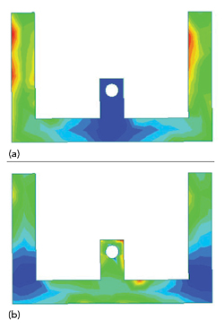
Figure 3 E-shaped resonator simulated E-fields: odd (a) and even mode (b).
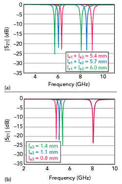
Figure 4 Simulated |S21| of the coupled E-shaped resonator vs. le1 + le2 (a) and le3 (b).