
A power divider is a basic microwave and millimeter-wave circuit dividing the input RF power by an arbitrary ratio. This circuit has a wide range of applications such as antenna systems, power amplifiers, power oscillators, balanced mixers and so on. Multiport power dividers/combiners have been used in power amplifiers to increase their output power.1
The Wilkinson type of microstrip power divider has been predominantly used as a multiport power divider. But λ/4 length transmission lines for impedance matching and parallel connection of resistors between output lines are required.2,3 If the resistor is eliminated in the power divider, a more efficient one-step fabrication process of the circuit can be accomplished.
Therefore, in order to develop a power divider without a resistor, a circular microstrip resonant structure had been suggested for the multiport circuit.4,5 Since this circuit had to have a coaxial feeding structure at the input, it was not easy to realize an all planar type circuit as required for MMIC or HMIC topology.
Next, even though a radial structure without the resistor had been introduced in planar form,6,7 there was a problem as the output lines were radially oriented, in which case the circuit area of the planar multiport structure was large. In general, for a smaller circuit area, the output lines should be oriented parallel with the input line.
To overcome the disadvantage of lines radially spread, new microstrip power divider geometries have been developed,8-10 having tapered contours for the external circuit edge, multiholes etched out from the circuit surface and where output and input lines were located in parallel orientation. This arrangement provided identical electrical length between input and multi-output ports.
The width of the microstrip power divider, however, has been monotonically increased from a 50 Ω input to an output plane connecting multi-50 Ω microstrip lines.
The design method given in the references8-10 has introduced an external contour geometry where the width is monotonically increased from input to output. For better input return loss, the physical width at the output plane should be narrower as the frequency is increased.

For example, at frequencies higher than 10 GHz, the discontinuity between the final transverse plane and the frequency-independent multi-50 Ω microstrip lines becomes small.
The width W2, in reference 10, at the output transverse plane should be maintained at approximately 0.6λ. If the number of output ports is increased, a width of approximately 0.5 to 1.0λ must be normally adopted. However, if this type of circuit contour is considered below approximately 10 GHz, the width W2 must be physically increased.
At 2 GHz, since the physical width at the output plane becomes wider, the discontinuity between the output plane and the multi-50 Ω microstrip output lines can be increased. When 1:2 and 1:3 power dividers at 2 GHz were designed by the method described in Kobeissi and Wu,10 10 and 11 dB return losses were shown as the best HFSS simulation results obtainable even if optimum tuning was carried out.

In order to overcome this problem, the contour geometry for the previously described multiport power divider8-10 has been modified.
Modification analysis has been carried out based on HFSS simulation. The modified geometry has an external shape such that the width at the output plane is reduced again after passing through a maximum width, located in the middle of the circuit. The frequency responses as a function of the circuit parameters of a practical circuit design have been included.
Based on these modifications, 1:2 and 1:3 power dividers have been developed for IMT-2000 at 2 GHz. The measurement results of the modified power dividers have been compared with the simulation results of the power divider designed by using the method of reference 10 at 2 GHz.
Modified Structure and Circuit Parameters
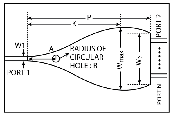
The modified structure of a planar multiport power divider is shown in Figure 1. The external contour of the power divider geometry is determined by Equation 1 that is identical to the one previously published,10 except for the denominator K in the cosine argument (K was P).
But K has been adopted in this study instead of P, to reduce the width at the output end of the microstrip power divider in which Wmax must be placed in the middle of the structure. Therefore,
where 0 <e; x <e; P and K must have a value between P and P/2. The final width of the structure, W2, is proportional to q. As the value of K becomes the center of the length of the structure, the output width, W2, approaches zero.
The circuit parameters of Equation 1, indicated in the diagram, are important factors in determining the external contour of the tapered geometry. In the following section, information for a practical circuit design will be given. After the circuit parameters for the geometry of a 1:2 power divider were extracted for the frequency range from 1 to 3 GHz through HFSS optimization, a 1:3 power divider was constructed by using the design parameters.
The frequency responses as a function of the circuit parameters P, K, q, A and R have been studied in terms of S-parameters for a 1:2 microstrip power divider structure which has been fabricated on a substrate with a dielectric constant εr = 10.2 and a thickness of 1.27 mm (Rogers RO 6010).
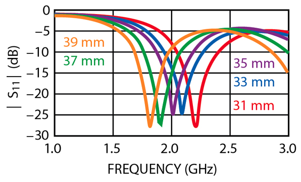
Figure 2 shows the center frequency variation (depending on the length P) of the modified structure for K = 0.4λ and q = 7. Table 1 summarizes the relationship between the center frequency and P expressed in electrical length. It has been observed that the length P is a circuit parameter determining the center frequency. Optimum characteristics have been obtained when the length was approximately 0.6λ.

K and q are the parameters for the location of Wmax and the width of the structure, respectively. The location and radius of a circular hole etched out on the structure can be chosen for better electrical characteristics.
Figure 3 shows the center frequency variation and the input return loss characteristics depending on q. Wmax and W2 increase with q. The discontinuity between the width at the output plane and the multi-50 Ω microstrip lines also increases with W2. In order to be operating at a 2 GHz center frequency for the 1:2 power divider, K = 0.4λ (23 mm) has been chosen.
|
Table 1 | ||
|
Length P |
Center |
Electrical |
|
31 |
2.209 |
0.600λ |
|
33 |
2.090 |
0.600λ |
|
35 |
2.015 |
0.601λ |
|
37 |
1.910 |
0.601λ |
|
39 |
1.821 |
0.601λ |
|S11| and the center frequency characteristics as a function of K are shown in Figure 4 .As the value of K approaches P/2 (longitudinal center of the structure), W2 becomes narrower. The center frequency variation can hardly be distinguished, but is improved by reducing K. K should be determined by considering the number of output port and electrical characteristics.
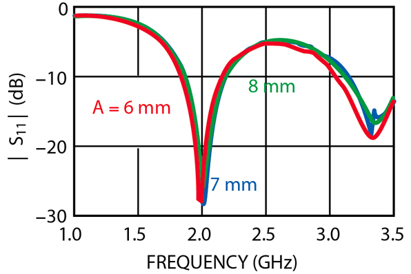
Figure 5 illustrates that the center frequency and input return loss characteristics depend on the values of A (6, 7 and 8 mm) when P = 0.6λ (35 mm), K = 0.4λ (23 mm), q = 1 and R = 1 mm. The location (A) of the etched circular hole has a negligible effect on the center frequency, but the characteristic is affected.
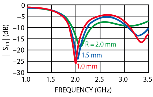
It has been found that as the radius R of the circular hole is increased, the center frequency moves higher and the characteristic is not improved, as shown in Figure 6 .
Based on this above analysis, the circuit parameters for the 1:2 power divider with the modified geometry have been determined at the center frequency of 2 GHz to be P = 0.6λ
(35 mm), K = 0.4λ (23 mm), Wmax = 0.31λ (17.86 mm), W1 = 1.12 mm, W2 = 0.16λ (8.98 mm), A = 0.12λ (7 mm), R = 1 mm and the width between output ports is 0.11 λ (6.4 mm). A 1:3 power divider with the modified geometry has also been designed and optimized at 2 GHz. In this case, the circuit parameters are P = 0.6λ (35 mm), K = 0.4λ (23 mm), Wmax = 0.32λ (18 mm), W1 = 1.12 mm, W2 = 0.25λ (14.6 mm), A = 0.13λ (8 mm), R = 1 mm and the width between output ports is 0.08λ (5 mm).
Result Comparison for the Modified Structure
The S-parameters of the 1:2 and 1:3 multiport microstrip power dividers have been simulated and measured with the εr = 10.2 and 1.27 mm thickness substrate as described before. The simulation for the previously described structure of reference 10 has been accomplished using the HFSS and measurements were carried out for the modified structure of this study.
The two results have been compared in the 1 to 3 GHz frequency range.
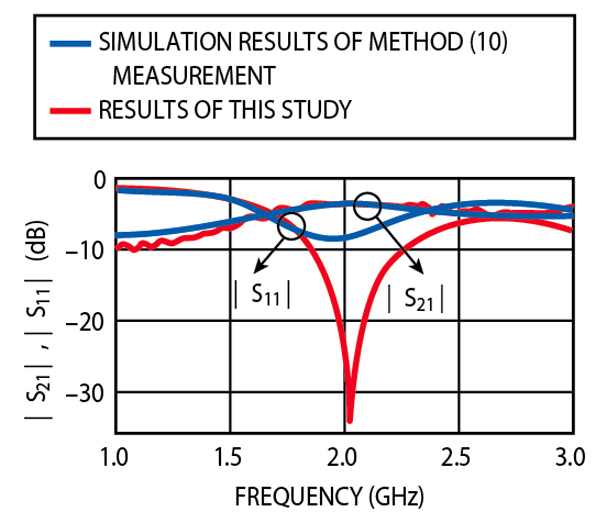
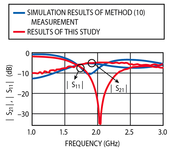
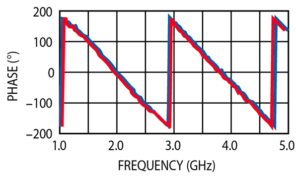
Figure 7 shows photographs of the modified 1:2 and 1:3 power dividers. Figures 8 and 9 illustrate the differences in S-parameters for the 1:2 and 1:3 power dividers developed by using the methods of Kobeissi and Wu10 and this study. For the 1:2 power divider, the difference in S21 between simulated and measured results is not easy to distinguish. However, the approach of this study provides a significant improvement of |S11|, from 9 to 33 dB. A similar improvement in |S11| has been obtained for the 1:3 power divider, from 10.5 to 37 dB. The phase characteristic of the 1:3 power divider with the modified structure is shown in Figure 10 , where a phase difference less than 1° between output ports has been obtained.
For a bandwidth characteristic based on a 20 dB return loss, this study has provided approximately 100 MHz for the 1:2 power divider and 120 MHz for the 1:3 circuit, but the structure simulated by the Kabeissi and Wu method10 could not be directly compared since |S11| characteristics better than 15 dB could not be achieved.
Conclusion
The external geometrical contour of the planar multiport power divider having parallel orientation of input and output lines8-10 has been modified for IMT-2000 application at 2 GHz. The circuit parameters for a practical design of the structure have been provided by HFSS analysis. Based on this analysis, 1:2 and 1:3 power dividers with the modified shape have been realized in microstrip form. S-parameter characteristics of the modified power divider have been measured and compared with simulation results of the 1:2 and 1:3 power dividers designed and optimized by the Kobessi and Wu method.10 This comparison shows that the modified power divider provides a significant improvement of the |S11| characteristic from 9 to 33 dB for the 1:2 power divider and from 10.5 to 37.0 dB for the 1:3 divider. For a bandwidth characteristic based on a 20 dB return loss, this approach has provided approximately 100 MHz for the 1:2 power divider and 120 MHz for the 1:3 circuit, but the structure simulated by the previously published method10 could not be directly compared since an |S11| characteristic better than 15 dB could not be achieved. By using the modified geometry, the physical circuit size has been reduced more than the one given by the previously published method.10
Acknowledgement
This work was supported in part by Grant No. R02-2001-00862 from the basic research program of the Korea Science and Engineering Foundation and by KyungHee University.
References
1. S.P. Marsh, "Power Splitting and Combining Techniques on MMICS," The GEC Journal of Technology , Vol. 15, No. 1, 1998.
2. A.A.M. Saleh, "Planar Electrically Symmetric N-way Hybrid Power Dividers/ Combiners," IEEE Transactions on Microwave Theory and Techniques , Vol. 28, No. 6, June 1980, pp. 555-563.
3. Y.J. Chen and R.B. Wu, "A Wide-band Multiport Planar Power Divider Design Using Matched Sectorial Components in Radial Arrangement," IEEE Transactions on Microwave Theory and Techniques , Vol. 46, No. 8, August 1998, pp. 1072-1078.
4. M.D. Abouzahra and K.C. Gupta, "Multiple-port Power Divider/Combiner Circuits Using Circular Microstrip Disk Configurations," IEEE Transactions on Microwave Theory and Techniques , Vol. 35, No. 12, December 1987, pp. 1296-1302.
5. M.D. Abouzahra and K.C. Gupta, "Multiple-port Power Divider/Combiner Circuits Using Circular Microstrip Disk Configurations," IEEE MTT-S International Microwave Symposium Digest , 1987, pp. 211-214.
6. M.D. Abouzahra and K.C. Gupta, "Multiport Power Divider/Combiner Circuits Using Circular Sector Shaped Planar Components," IEEE Transactions on Microwave Theory and Techniques , Vol. 36, No. 12, December 1988, pp. 1747-1751.
7. M.D. Abouzahra and K.C. Gupta, "Use of Circular Sector Shaped Planar Circuits for Multiport Power Divider/Combiner Circuits," IEEE MTT-S International Microwave Symposium Digest , 1988, pp. 661-664.
8. Q.C. Sun, K.W. Eccleston and S.P. Yeo, "The Design of Optimum Planar Power Divider/Combiner for SSPA Applications," 1995 Asia Pacific Microwave Conference, South Korea, December 1995, pp. 499-505.
9. J. Benbrahim, H. Kobeissi and K. Wu, "CAD and Electrical Performance of a New Compact Power Divider Suitable for Use in M(H)MICs," IEEE MTT-S International Microwave Symposium Digest , June 1997.
10. H. Kobeissi and K. Wu, "Design Technique and Performance Assessment of a New Multiport Multihole Power Divider Suitable for M(H)MICs," IEEE Transactions on Microwave Theory and Techniques , Vol. 47, No. 4, April 1999, pp. 499-505.
Yongin Han received his BE and MAS degrees in electrical engineering from KyungHee University, Suwon, South Korea, in 2000 and 2002, respectively. He is currently working for Sewon Telecom, Seoul, as a research engineer. His research interests are in the areas of power dividers/combiners, microwave oscillators and RF part design in CDMA PCS phone.
Ihn S. Kim received his BE degree in electrical engineering from KyungHee University, Suwon, South Korea, in 1974, and his MAS and PhD degrees, both in electrical engineering, from the University of Ottawa in 1983 and 1991, respectively. He has worked for the Canadian Space Agency, Com Dev Ltd., General Instrument of Canada and the Korean Broadcasting System. From February 1999 to February 2000, he was on sabbatical at ETRI (South Korea), ETH (Switzerland) and Motorola Florida Research Lab (US). He is currently a professor teaching microwave engineering in the school of electronics and information at KyungHee University. His research involves commercial application of radar technology, modeling of microwave structures by numerical methods (FEM, FDTD and TLM) and their application to filters and power divider/combiners, and nonlinear microwave circuit development such as oscillators and mixers. He can be reached via e-mail at ihnkim@khu.ac.kr or by phone at +82-31-201-2587.