
High-power transistors are formed from a group of smaller transistor cells, paralleled on a single die or in a package, to achieve the highest output power possible. As packaging and testing dominate manufacturing cost, power is “squeezed” into the package for highest cost-effectiveness. This gives the most “bang per buck,” typically measured in dollars per watt. However, while increasing the power in a single package reduces device cost per watt, it lowers system efficiency through many subtle effects:
- Densely packed power transistor cells do not play well together: collocating the smaller power cells reduces thermal performance and efficiency.
- The layout of the cells must be optimized for all cells to contribute equally to the output power. The inner transistor cells run hotter, creating undesirable hot spots that reduce the cell’s power.
- The optimum load impedance decreases monotonically as the transistor gets larger, becoming difficult to match into the typical 50 Ω system over a broad bandwidth. The associated low impedance bias tee becomes large and lossy and can significantly affect the output matching.
- Often, on-chip impedance matching is used to increase the optimum external load impedance to more practical levels, easing the design task for the board designer. However, the in-package matching has as much loss as doing the transformation externally.
THE SYSTEM VIEW
From a system perspective, the bang - the output power performance - is measured at the system output, not at the device. The buck - the total cost - includes cooling and the total DC power consumption. What is optimum for the device is not necessarily optimum for the system. A different bang per buck perspective for power amplifier (PA) design prioritizes increasing system efficiency and eliminating heat as the drivers determining the buck, where device bang is reduced to a “bong” by the combining efficiency. This is illustrated by the following 240 W PA example, where the conventional combiner design results in 600 W total dissipation, and the Werlatone combiner dissipates only 400 W.
CURSE OF THE 50 Ω INTERFACE
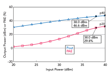
Figure 1 Output power and PAE vs. input power at 500 MHz, with the device output matched using three N-squared transformer stages.
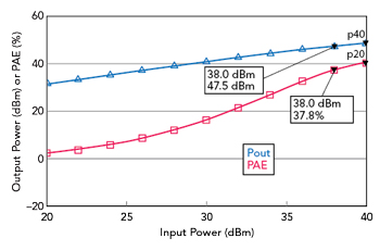
Figure 2 Output power and PAE vs. input power at 500 MHz, with the device output matched to a 12.5 Ω four-way combiner using a single non-N-squared transformer stage.
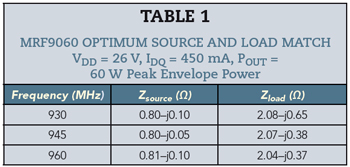
A 60 W LDMOS power transistor is selected for the design of a 240 W PA at 500 MHz. To achieve the highest output power and power-added efficiency (PAE), the optimum source impedance and output load for the NXP MRF9060 transistor are shown in Table 1. The real parts of the source and load match are 0.8 and 2 Ω, respectively. Consider the following two approaches to matching the output:
Conventional Design - Each 60 W device will be matched to 50 Ω using N-squared transformers, then combined with a four-way 50 Ω combiner to achieve a nominal 240 W. This approach requires three stages of N-squared transformers to transform from 2 to 50 Ω, which incurs 1.2 dB of insertion loss, assuming a typical insertion loss of 0.4 dB per stage. This impedance transformation reduces the output power of each MRF9060 to 46.6 dBm (45 W) from the specified 47.8 dBm (60 W) and the PAE is reduced to 29.8 percent from the specified 40 percent. The four-way 50 Ω combiner adds 0.8 dB insertion loss, making the total output power of the PA 51.8 dBm (151 W) at 25.2 percent efficiency, with a thermal dissipation of 449 W. The resulting power and PAE performance are shown in Figure 1.
Alternative Design - Using a Werlatone 12.5 Ω combiner, the transistor is matched to 12.5 Ω, rather than 50 Ω. As the sum port on the combiner is at 50 Ω, combining four of the 60 W amplifiers is straightforward. With this architecture, only a single stage of a non-N-squared transformer is needed, which adds 0.3 dB insertion loss and reduces the output power of the MRF9060 to 47.5 dBm (56 W) from its specified 47.8 dBm (60 W). The PAE decreases to 37.8 percent from the specified 40 percent. The four-way 12.5 Ω combiner adds 0.5 dB insertion loss, further reducing the output power to 53 dBm (200 W) at 33.3 percent efficiency, with a thermal dissipation of 400 W. The power and PAE of the 240 W PA design using this approach are shown in Figure 2.
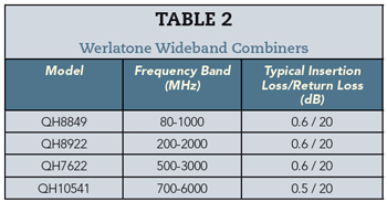
With the conventional design, achieving 200 W output power would result in 600 W thermal dissipation. The alternative design approach reduces the loss by using impedance transforming combiners, which have less loss than four-port 50 Ω combiners. This has inspired Werlatone to design a family of input power combiners with interface impedances of 8 or 12 Ω and an output sum port of 50 Ω. Table 2 shows a partial list of these combiners, illustrating the bandwidth capability Werlatone can provide. Various customized versions, with the port impedances set to customer requirements, can readily be designed, up to input-sum port impedance ratios as high as 4:1 referenced to 50 Ω over bandwidth ratios of 10:1.
SUMMARY
Werlatone’s product line of transforming impedance combiners -- 12.5 Ω input and 50 Ω output featured in this article, but customizable to other impedances -- greatly improves PA PAE by reducing transformer and combiner losses. Should more power be needed, additional transforming combiners can be used to quadruple the power with little additional combiner loss. Where an unusual impedance transformation is needed, no compromise is necessary with Werlatone’s non-N-squared transformer techniques.
Werlatone Inc.
Patterson, N.Y.
www.werlatone.com
(845) 278-2220