It is shown both theoretically and by simulation that a balanced amplifier has a lower VSWR withstand capability than that of the transistors used in its construction, meaning the maximum VSWR before the transistor will fail or its reliability degraded. A revised VSWR withstand capability should be adopted for a balanced amplifier to prevent device failure.

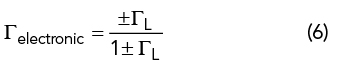
Figure 1 Different physical and electronic loads seen by an amplifier.
High power amplifiers often require the combining of multiple transistors. This can be done using in-phase combining with Wilkinson or Gysel combiners, anti-phase combining (i.e., push-pull) with baluns or quadrature combining (i.e., balanced amplifiers) with quadrature or hybrid couplers (e.g., branch-line or Lange). The combining structure determines the amplifier’s ability to withstand large VSWR mismatches, which affects the amplifier’s ruggedness and reliability. Other methods may be used for power combining, in addition to the three noted above, such as serial combining1 and traveling-wave combining,2 but these are seldom, if ever, used when combining just two transistors.
In-phase combining provides the same VSWR withstand capability as for each individual transistor, disregarding losses through the combiner. Considering the fundamental properties of the scattering matrix of a lossless, reciprocal, three-port network, such as a balun, a push-pull amplifier also has the same VSWR withstand capability as the individual transistors. The situation for a balanced amplifier, however, is more complex and is the focus of this article.
IMPACT OF VSWR
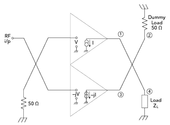
Figure 2 Balanced amplifier.
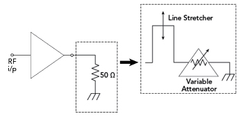
Figure 3 Setup for measuring the VSWR withstand capability of an amplifier.
A balanced amplifier consists of two identical amplifiers operated in-phase quadrature. A quadrature coupler or splitter creates a 90 degree phase difference between the signals applied to the two amplifiers. A second quadrature coupler at the output removes this phase differential, so the amplifier outputs combine in phase.3 One of the advantages of a balanced amplifier is it provides excellent VSWR at the external terminals, even if the two internal amplifiers have poor terminal VSWRs.
This article examines the converse problem, namely determining the VSWR presented to the two internal amplifiers - hence transistors - when a mismatch is presented at the amplifier’s external port. An analytical calculation is made of the VSWR presented to the active devices of a balanced amplifier, and the results are verified through simulation using Cadence®AWR Design Environment® software. In the presence of a mismatch at the amplifier output, one amplifier or transistor, sees an improved VSWR and the other is subjected to a larger mismatch. From a priori knowledge of the transistor’s VSWR withstand capability, one can determine the impact of impedance mismatch on the ruggedness and reliability of the balanced amplifier.
PREVIOUS WORK
Determining the VSWR presented to the two internal amplifiers when a mismatch is presented at the balanced amplifier’s external port has been previously considered by both Cripps4 and Raab.5 Cripps’ analysis remains unpublished while Raab used a combination of a Ruthroff transformer and a balun to create a quadrature hybrid, a concept probably unfamiliar to most microwave engineers. Raab’s and Cripps’s analyses, however, are in total agreement with the results presented here.
The problem was considered more recently by Jung et al.6 However, their analysis calculates the value of the physical load that each internal amplifier sees, not the value of the electronic load; so their analysis cannot determine the VSWR withstand capability of a balanced amplifier. The significance is illustrated in Figure 1. Each current generator sees a physical load of 1 Ω, but the voltage across the resistor is 2 V. Hence, each current generator sees an electronic load of 2 Ω, rather than 1 Ω. In the case of the balanced amplifier (see Figure 2), it is essential to calculate the load seen by each amplifier while both amplifiers are simultaneously injecting current into the coupler, i.e., the electronic load.
MEASUREMENT OF VSWR WITHSTAND CAPABILITY
The traditional method of measuring VSWR withstand capability is to steadily increase the RF input power to the transistor in a test fixture until the RF output power reaches its full rated value. The load is then replaced with an attenuator terminated in a short circuit and preceded by an adjustable transmission line stretcher or suitable phase shifter (see Figure 3). The line stretcher is adjusted to sweep the phase of the load through 360 degrees. The attenuation is then reduced in stages and the process repeated until the transistor fails. Strictly speaking, this method measures the VSWR withstand capability of the transistor in its particular test fixture, including any losses from the test fixture’s output matching network. As the losses in the output network are normally minimized to maximize amplifier efficiency and output power, this method does actually determine the VSWR withstand capability of the transistor to a good approximation. The VSWR withstand capability is quoted with reference to a 50 Ω load and not the load impedance the transistor sees.
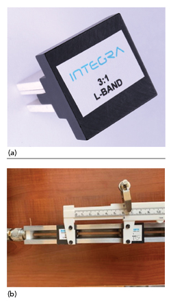
Figure 4 3:1 VSWR slug (a) and 2:1 and 5:1 slugs cascaded λ/4 apart to present 10:1 VSWR (b).

Figure 5 Equivalent network seen by the two amplifiers.
An alternative method of measuring VSWR withstand capability more suitable for a production environment is to insert at least a wavelength long slot line between the test fixture and the load, then insert a quarter-wave impedance transformer - commonly referred to as a slug - which can be slid along the length of the slot line. The slug is created by inserting an appropriate length section of dielectric between the center and ground conductors (see Figure 4a). The thickness and dielectric constant are chosen to give the required VSWR mismatch; for example, a slug with 2:1 mismatch has an impedance of 35 Ω.
For normal testing of power, efficiency and gain, the slug is not inserted and the small residual loss of the air filled slot line is calibrated out. The advantage of this measurement method is that no dismantling and reconstruction of the test bench is required, and VSWR withstand testing can be incorporated as a standard part of production testing. Figure 4b shows an Integra L-Band GaN transistor being tested for VSWR withstand with a 10:1 mismatch, created by cascading 2:1 and 5:1 slugs spaced a quarter wavelength apart.
These two techniques are not equivalent. In the first method, the mismatch presented to the transistor is constant at all frequencies. In the second, the same mismatch is presented at the fundamental and all odd harmonics, but a 50 Ω load is presented at the even harmonics. In most situations of practical interest, the two techniques give essentially the same result.
BALANCED AMPLIFIER VSWR WITHSTAND CAPABILITY
The scattering matrix (S-matrix) of an ideal quadrature coupler at band center is given by
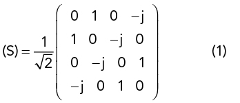
where the port numbers of the hybrid coupler are defined in Figure 2. For a balanced amplifier, the two internal amplifiers see a two-port network formed by the directional coupler, with port 2 terminated in a 50 Ω load, providing a reflection coefficient of Γ = 0, and port 4 terminated in a variable load with a reflection coefficient of Γ = ΓL. The two-port network has a scattering matrix given by
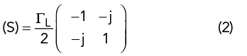
The S-matrix of equation (2) can be converted to a Z matrix, given by
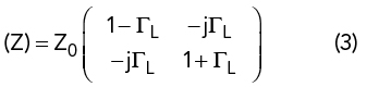
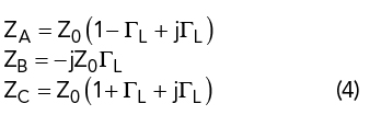
At band center, the two amplifiers see the simple equivalent two-port network shown in Figure 5, where the element values are given by
To this point, no assumption is made about the amplitude or phase relationship of the signals applied to ports 1 and 3 in Figure 5. If the amplifiers are assumed ideal and consist of just a current generator, as shown in Figure 2, the electronic load seen by the two transistors is given by

which, when expressed as a reflection coefficient, is given by