

Consequently, while one transistor sees an improved VSWR, the other sees a worse VSWR.
To demonstrate the impact of the electronic load on amplifier ruggedness and reliability, consider a balanced amplifier with each transistor having a VSWR withstand capability of 5:1, i.e., |Γelectronic| = 0.66. From equation 6, the maximum VSWR withstand capability of the balanced amplifier at the load port is only 2.3:1, i.e., |ΓL| = 0.39.
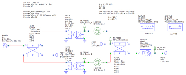
Figure 6 Simulating an ideal balanced amplifier with swept load impedance.
These results are verified using circuit simulation with an ideal hybrid coupler model and voltage-controlled current source models to represent the balanced amplifier in a virtual test setup with a variable load impedance, typically used in load-pull simulations. Figure 6 shows the simulation schematic in the AWR® Microwave Office® circuit simulator. Figure 7 shows the reflection coefficient seen by the two transistors. The magnitude of the reflection coefficient at the load is fixed at a gamma equivalent to a 2.3:1 VSWR, while the phase is varied from 0 to 180 degrees in 7.5 degree increments. The simulation agrees with the theory predicted by equation 6.
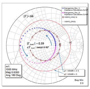
Figure 7 Reflection coefficient seen by the two transistors with a fixed |ΓL| = 0.39 and swept ∠ΓL from 0 to 180 degrees.
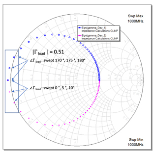
Figure 8 Negative resistance at the transistor ports for |ΓL| >0.50 and swept ∠ΓL <10 degrees or >170 degrees.
With a mismatch, one of the transistors will experience a higher mismatch than seen at the output to the balanced amplifier, potentially exceeding the transistor’s VSWR withstand rating for maximum power output. From equation 5, if the external mismatch exceeds 3:1 (i.e., |ΓL| = 0.5), one of the transistors may see a negative resistance depending on the phase of ΓL (see Figure 8). While a mathematically correct deduction, this will not arise in practice unless the transistor can survive an infinite VSWR mismatch, as the transistor will already have failed at a lower value of external VSWR mismatch. However, one of the transistors may see a negative resistance under small-signal conditions in the presence of an external mismatch, which may cause instability.
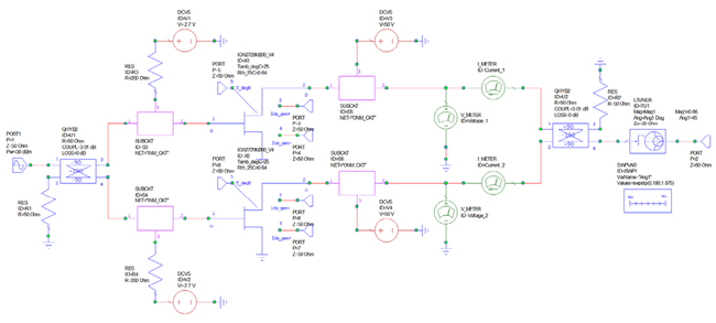
Figure 9 Simulating a balanced amplifier using the IGN2729M200 devices.
REALISTIC TRANSISTOR MODEL

Figure 10 VSWR circle and loads seen by each side of the balanced amplifier under a 5:1 output mismatch, as the phase of the external mismatch is rotated through 180 degrees.
The previous analysis uses a simple model for the transistor and amplifier, resulting in a simple expression to illustrate the problem. The analysis is repeated using real amplifier and transistor models. The IGN2729M200 is a 2.7 to 2.9 GHz transistor capable of delivering 200 W output power over this frequency range with a 100 µs pulse length and 10 percent duty cycle. Integra’s full nonlinear electrothermal model for this device was used and embedded within a model for the input and output matching networks of the two amplifiers. The quadrature coupler is assumed to be an ideal lossless device with a center frequency of 2.8 GHz. Figure 9 shows the Microwave Office circuit schematic, which may be compared with the simplified model shown in Figure 6.
Figure 10 shows the reflection coefficient seen by the two internal amplifiers as the phase is swept from 0 to 180 degrees and a 5:1 VSWR mismatch is applied to the balanced amplifier’s output port. As before, one amplifier or transistor sees an improved mismatch while the other sees a considerably worse mismatch - in this case as high as 10:1 at some phases of the external mismatch.
CONCLUSION
In this article, the VSWR withstand capability of a balanced amplifier was calculated and verified through simulation, showing a balanced amplifier has a lower VSWR withstand capability than the individual transistors used in its construction. This should be accounted for in the design of a balanced amplifier to prevent device failure.
References
- K.J. Russell, “Microwave Power Combining Techniques,” IEEE Transactions on Microwave Theory and Techniques, Vol. 27, No. 5, May 1979, pp. 472–478.
- A.G. Bert and D. Kaminsky, “The Travelling-Wave Divider/Combiner,” IEEE Transactions on Microwave Theory and Techniques, Vol. 28, No. 12, December 1980, pp. 1468–1473.
- K. Kurokawa, “Design Theory of Balanced Transistor Amplifiers,” Bell System Technical Journal, Vol. 44, No. 8, October 1965, pp. 1675–1698.
- S.C. Cripps, private communication.
- J.L.B. Walker, D.P. Myer and F. H. Raab (Editors), “Classic Works in RF Engineering: Combiners, Couplers, Transformers and Magnetic Materials,” Artech House, 2006.
- I. Jung, M. Seo, J. Jeon, H. Kim, M. Cho, H. Lee and Y. Yang, “Analysis on the Balanced Class-E Power Amplifier for the Load Mismatch Condition,” Semantic Scholar, 2012, Web. https://www.semanticscholar.org/paper/Analysis-on-the-Balanced-ClassE-Power-Amplifier-for-Jung-Seo/179657496159b462bd2e6dcd7b2b2cf51de5b99c.