

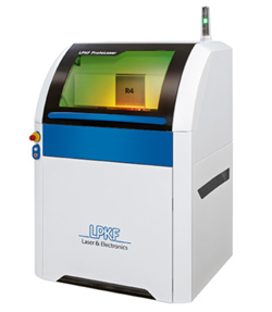
Figure 1 LPKF ProtoLaser R4.
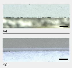
Figure 2 GaN edge after dicing (a) and laser cut (b).
Metal plated GaN-based ceramic materials with a thin metallic conductor layer on a thick, brittle ceramic base, pose an intriguing challenge for material processing. The LPKF ProtoLaser R4 system can quickly and cleanly process both material layers, regardless of the specifications and stark contrast in their material properties. The ProtoLaser R4 offers accuracy, adaptability and tunability.
Novel materials and advances in material processing technologies have pushed innovation since ancient times. Current trends include using GaN-based chips and interconnects, rather than silicon, for power electronics and RF/microwave components for radar, electronic warfare, 5G and satellite communications.
Commonly, GaN ceramic is the substrate material and covered with thin metal layers, typically micrometer-thick gold. Material processing includes dicing the ceramic substrate and etching the metal layer, traditionally two separate steps. The goal of laser-based processing using the LPKF ProtoLaser R4 system (see Figure 1) is integrating the two manufacturing steps into a single contactless and chemical-free step. While contactless and chemical-free processing are properties of all laser machining procedures, the ProtoLaser R4 system implements an ultra-short pulsed laser source capable of achieving or surpassing the tolerances of the traditional manufacturing steps. The ultra-short pulses and machine design eliminate the need for final cleaning of the material, yielding fast processing times for small batch production or individual samples.
PROCESSING STEPS
The first step of the laser processing procedure is cutting the outline of the desired sample in the ceramic. The top gold layer acts as a shield against accumulated heat and the ejected plasma, protecting against cracks and chips forming in the ceramic substrate. As traditional dicing techniques offer a trusted level of edge quality, the laser process strives to achieve - even improve - this performance.
An important aspect of laser cutting is maximizing efficiency: the amount of laser energy delivered into the material per surface area and per unit time must be carefully optimized and constantly controlled. Optimizing processing efficiency provides both the highest speed processing and the lowest thermal impact to the surrounding material and works in the so-called cold ablation regime. This is only achievable with the optimized application of ultra-short laser pulses, which the ProtoLaser R4 provides.
Figure 2 compares the edge quality of the ceramic using dicing and the laser process. With the laser, cracks and chips are virtually nonexistent. Where dicing produces a taper-free cut, laser cutting solid materials intrinsically creates a V-shaped, tapered channel, with a small difference between the top and bottom dimensions. This tapered edge does not affect the functional properties in any way. Optimizing the laser cut for cosmetic appearance and to minimize the taper results in approximately 0.1 mm taper for a 0.25 mm thick ceramic. For example, if the top side length is 10.0 mm, the bottom side length will be 10.1 mm.
After cutting, the sample is held firmly in place by the ProtoLaser R4 vacuum table, and no user intervention is required to proceed to the second step. The laser output power is reduced, tuned to the thin top layer of metal. In contrast to the high power, high pulse energy used to cut the ceramic, the laser now emits low power, low energy pulses for etching the top gold. At low energy, the size of metal structures and the spacing between them can be comparable to the size of the laser beam, which has a spatial Gaussian profile. The ProtoLaser R4 provides a beam spot size as low as 15 μm, enabling laser etched metal layers to have features as small as 15 μm with equally small spaces between them (see Figure 3). The smallest features are largely determined by the thickness of the metal layer, which is thin compared to the lateral dimension of the structure, and the uniformity of the layer.
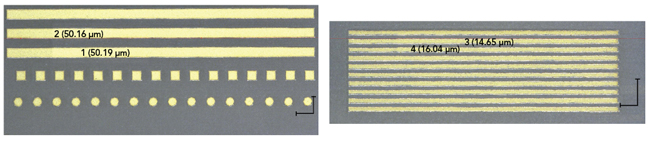
Figure 3 Uniformity of gold metallization etched with the laser.
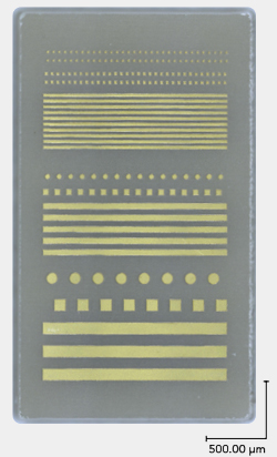
Figure 4 GaN sample, including rounded edges, processed with the LPKF ProtoLaser R4.
Whether using chemical etching techniques or laser processing, the ability to achieve finely spaced structures is a function of the material properties, device design and the processing parameters. Important processing considerations include the design features, both curves and straight lines; minimizing damage to the substrate; and clean removal of debris. Using the laser, debris-free processing is achieved with the ProtoLaser R4’s air flow chamber; ultra-short pulsed ablation, which ejects very small particles; and the energy input per surface area.
Figure 4 shows the finished experimental sample. The small size of the sample is a handling challenge for traditional cutting techniques, but the laser has no trouble - even adding rounded corners to the design to demonstrate the ability to create shapes with irregular outlines.
SUMMARY
As demonstrated, the LPKF ProtoLaser R4 provides a single-step manufacturing procedure for cutting and etching plated GaN ceramic structures. The optimized ultra-short pulsed laser processing enables fast, clean, precise, chemical-free processing with a user-friendly approach, supporting applications demanding tight tolerance, reliable output and fast turnaround to accommodate frequent design changes. This application is just one of the ProtoLaser R4’s rather unique applications, which include cutting, drilling and structuring typical RF/microwave materials, PTFE, double-sided flexible PCB laminates and thin metal layers on glass.
LPKF Laser & Electronics AG
Garbsen, Germany
www.lpkf.com