
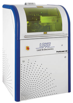
The UV laser is widely regarded as a universal tool for material processing. So, it is significant that the new LPKF ProtoLaser U3, that is suitable for the laboratory, can now also structure laminated printed circuit board substrates, expanding the already broad line-up of materials to include this important application.
Laminated Substrates
Laser systems have been playing an important role in this area for several years. In a patented process, the ProtoLaser S structures laminated substrates using a laser with a wavelength of 1064 nm. The laser beam first separates the strip conductors, then hatches the rub-out surfaces and subsequently removes the hatched metal strips.
The UV laser system previously available for prototyping is positioned very differently. It processes a broad range of materials, separates flexible and thin rigid printed circuit boards, structures invisible TCO coatings, cuts ceramic and exposes metal resists for production of ultra-fine conductors. However, up until now, laminated materials could not be handled by this system.
That has changed with the introduction of the ProtoLaser U3, which combines the capabilities of both ProtoLaser systems into one universal tool. This system is a good example of the wide range of laser technology when the mechanical components, the control systems and the machine software work well together. The laser source used is a proprietary development in the 355 nm range. It operates with a typical output of 5 to 6 W and works in a frequency range of 10 to 200 kHz. With a focus diameter (spot size) of 15 µm and a scanner resolution of 2 µm on the material, the system is also designed for the processing of ultra-fine structures.
Just like the previous UV system, the ProtoLaser U3 processes the entire range of materials and in addition, handles the structuring of laminated substrates. This system can thus carry out a whole series of tasks in printed circuit board prototyping:
Structuring: building up the desired conductor network from substrate plates that are coated all over (see Figures 1 and 2).
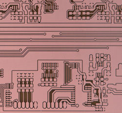
Fig. 1 Structuring of laminated substrates, e.g., FR4, takes place in an isolation process: the laser beam separates the desired conductor tracks from the surrounding copper.
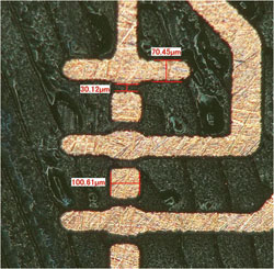
Fig. 2 With a pitch of only 100 µm, this prototyping process is more precise than many serial processes.
Drilling: by cutting holes with exactly defined diameters, holes or blind holes can be created. The penetration depth of the laser beam can be controlled very precisely by the number of repetitions.
Embedding of components in the printed circuit board: the UV laser cuts the recesses or, in the case of multilayer printed circuit boards, the holes in which components are positioned are flush with the surface.
Decap: rigid-flex printed circuit boards are produced in manufacturing as ‘sandwiches’ of various substrate materials. The UV laser beam cuts out the rigid elements in areas that are to be flexible in the end product.
Depaneling: the UV laser detaches individual printed circuit boards from the larger base material. In the process, neither mechanical nor thermal damage occurs, and even irregularly shaped contours are no problem for the scanner-controlled laser beam.
Cutting prepreg and cover layers: both materials are flexible and sensitive to distortions. In laser processing, a vacuum table takes over the fixing while the laser beam is responsible for contactless processing without mechanical strain.
On laminated materials such as FR4, distances and lines of 30/70 µm can still be created without damaging the sensitive substrate. For this type of structuring, LPKF includes a special hood for the laser processing head.
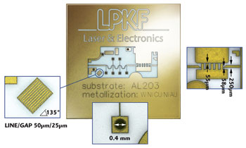
Figure 3 Highly precise structures on a small coated ceramic plate with dimensions of 25 × 25 mm.
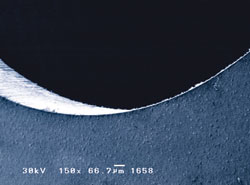
Figure 4 Precise cuts: The UV laser beam separates sensitive ceramic materials. Shown here is Al2O3.
Processing ceramic materials
Fig. 5 Suitable for harsh environments: The ProtoLaser U3 structures, engraves and cuts LTCC components in one pass.
The suitability of the UV laser system for processing ceramics is an important consideration. A core capacity of laser processing is structuring high-quality RF circuitry, e.g., gold on ceramic. The material compounds are sensitive to mechanical actions and geometric deviations, are expensive and cannot be processed adequately with conventional tools. The solution is a laser system that vaporizes tiny amounts of gold coating pulse by pulse and leaves the metalized network structure of the circuitry unaffected, as illustrated in Figure 3.
The UV laser is also impressive in separating ceramic with a clean cut edge, as shown in Figure 4. The versatility of the system is demonstrated again with the example shown in Figure 5 – in a single step, the UV laser structures the LTCC pattern, cuts circles inside, engraves the marking and separates the entire component with an irregular contour from the truss.
The compact system has a footprint of only 875 by 750 mm, meaning it can be transported and sited in laboratories easily; wheels make it readily moved to wherever it is needed. It requires only one power connector, a dust extractor and a compressed air connection, with the compressed air playing a decisive role in the removal of metal strips.
Quick prototyping reduces the time it takes to launch a product to the market. Being able to produce series-like prototypes and small batches independently ensures that confidential data does not leave the development lab. This is often an important criterion for companies. The LPKF ProtoLaser U3 addresses these issues and when it comes to quality, the UV laser in combination with capable CAM software offers significant advantages.
LPKF Laser & Electronics AG,
Garbsen, Germany
+49 5131 7095 0,
info@lpkf.com,
www.lpkf.com.