
Technical Feature
Measurement of On-wafer Transistor Noise Parameters Without a Tuner Using Unrestricted Noise Sources
This article presents a method for calibrating the four noise parameters of a noise receiver which does not require a tuner. The method permits using general (mismatched) noise sources, which may present very different source reflection coefficients between their hot and cold states. The method is applied to the calibration of a noise set-up using on-wafer noise sources (a reverse-biased cold-FET and an avalanche noise diode). Experimental validation of the receiver calibration and its application to the determination of on-wafer FET noise parameters to 40 GHz is presented.
A. Lázaro, M.C. Maya and L. Pradell
Universitat Politècnica de Catalunya (UPC)
Barcelona, Spain
An accurate knowledge of transistor noise parameters (NP) is essential to the design of low noise amplifiers (LNA). Before the NPs of the device-under-test can be measured, the noise receiver must be calibrated. Calibration consists of the determination of the four receiver NPs. Conventional calibration techniques require measurements of noise powers presented at the receiver input for a number of reflection coefficients produced by a broadband tuner.1 However, this technique is costly and time-consuming. An alternate method2 permits determining the receiver NPs from 50 W noise-figure measurements, by using a commercial, well-matched coaxial noise source. This method has demonstrated an accuracy comparable to that obtained by using tuner-based methods.
While a matched source is the noise reference most commonly used, it has been shown3 that an on-wafer diode noise source is a convenient noise reference to calibrate the receiver for measuring NPs of on-wafer transistors directly. However, on-wafer diode noise sources are highly mismatched devices and their reflection coefficient varies significantly between the hot and cold states. Therefore, the previously proposed method2 to calibrate the receiver cannot be applied, because it assumes that the receiver noise-figure does not change noticeably between both noise source states. An on-wafer attenuator pad to achieve a broadband matching condition is normally introduced after the noise diode,3 but this lossy pad has the drawback of reducing the effective level of excess noise ratio (ENR) at the on-wafer reference-plane.
Alternatively, this work presents a novel method to calibrate the noise receiver with a general (mismatched) noise source and does not require a tuner, which adds flexibility to the design of new types of noise sources, specifically on-wafer noise sources. There is no restriction on the variation of the source reflection coefficient between the hot and cold states, and the receiver noise-figure need not be constant for both noise source states. To verify the method, calibration results are compared to those obtained with a tuner-based method,1 and the NPs of a passive semiconductor device (common-gate, on-wafer, cold transistor) are measured and the results are compared to those derived from its S-parameters. The proposed method is used to calibrate the noise receiver with mismatched on-wafer noise sources and applied to the determination of the NPs of FETs. The experimental results are presented in two bands, 2 to 22 GHz and 26 to 40 GHz.
Fig. 1 Noise figure and nosie parameter measurement system.
Experimental Set-up
Figure 1 shows the experimental set-up. It is a typical configuration for the determination of on-wafer transistor noise parameters, but without the inclusion of a tuner. It consists of the following components: A VNA (HP8510C) for calibration and measurement of the set-up reflection coefficients and the device-under-test (DUT) S-parameters; a test fixture for inserting the DUT - a wafer-probe station (SUMMIT-9000 from Cascade-Microtech) is used; three remotely controlled coaxial switches (SW) to select between the lower and the upper noise measurement bands (2 to 22 GHz and 26 to 40 GHz, respectively), and between VNA and noise measurements; two bias-tees; noise sources - in this work, two on-wafer noise sources (OWNS) and one coaxial (HP346C) noise source are used; a noise receiver composed of a spectrum analyzer (SA) (HP70000 series), a low noise amplifier (LNA) for the lower frequency band (2 to 22 GHz) to reduce the SA noise-figure, a low noise block downconverter (LNB-2642-50 from MITEQ), which includes an input LNA to convert the upper frequency band (26 to 40 GHz) into an IF range (5 to 19 GHz) within the SA range, and an external detector connected to the SA 21.4 MHz IF output. All measurements are automated and controlled with an external PC via GPIB.
Fig. 2 Receiver equivalent wave noise sources bn1 and bn2 .
Method for Receiver Calibration With Unrestricted Noise Sources
Since the LNAs in the receiver front-ends are basically unilateral devices, their scattering noise-matrix representation4 can be simplified by assuming that their equivalent wave noise sources bN1 , bN2 (see Figure 2 ) are uncorrelated
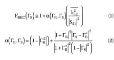
Under this hypothesis, the receiver noise-figure FREC can be approximated by5
where
GS = source reflection coefficient
Since the LNAs are basically unilateral, it has been also assumed in Equations 1 and 2 that S11 » GR , where GR is the receiver input reflection coefficient and S11 , S21 are the receiver S parameters. The impact of such hypothesis on the determination of the receiver noise parameters (in particular Fmin and Rn ) is discussed later. Note that a(GR , GS ) is a quantity that only depends on the reflection coefficients measured with the VNA. To determine the normalized noise power wave
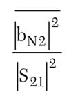
the noise powers delivered to the receiver for two states (hot and cold) of the noise source, PHOT and PCOLD respectively, are measured. Then the following ratio R of noise powers available at the plane 2-2' can be computed
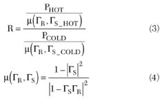
where
m(GR ,GS ) = mismatch coefficient that only depends on reflection coefficients
GS_COLD = cold source reflection coefficients
GS_HOT = hot source reflection coefficients
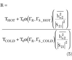
Then, the power ratio R is written in terms of the receiver noise temperature TREC = (FREC -1) T0, where FREC is given by Equation 1 and T0 is the standard temperature (T0 = 290K), as
where
THOT = noise source hot temperature
TCOLD = cold temperature (room temperature)
From Equation 5, the quantity
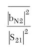
is computed as
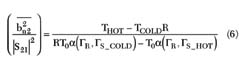
Using Equation 6, the receiver NPs are readily computed assuming the same approximation made previously for the receiver
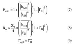
where
Z0 = normalizing impedance
It is assumed in Equation 9 that the LNA has been designed for minimum noise.
Note that, in contrast with previous methods2 , significant variations in the receiver noise-figure due to different hot and cold noise source reflection coefficients are allowed and taken into account in Equation 6 through the quantity a(GR , GS ) defined in Equation 2. Furthermore, the noise device which provides the hot state temperature (THOT ) may be physically different from the device at cold temperature (TCOLD ). In this work, examples of calibration using on-wafer noise sources for the hot state and a coplanar 50 W load for the cold state are given.
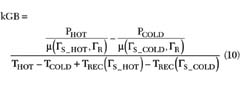
Finally, the receiver gain-bandwidth constant kGB (where G is the receiver transducer gain for GS = 0, and B is the noise measurement bandwidth) must be determined using
After calibration, the noise-figure of an arbitrary DUT can be obtained as follows. The total noise-figure (DUT plus receiver) for a measured reflection coefficient at plane 1-1' (Gs ') computed from the measured noise power P(GS ') is

where
GOUT = DUT ouput reflection coefficient
Tf = physical temperature of the source termination (typically, room temperature)
GDUT = DUT available gain
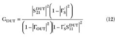
The DUT noise-figure is obtained using Friis' formula
Finally, assuming that the DUT is an on-wafer FET, its measured noise-figure (Equation 13) is applied to determine the FET noise parameters using the method proposed in reference.6 This method (so-called F50 ) is based on the determination of the FET intrinsic noise-matrix elements by frequency-fitting the measured device noise-figure for a known source reflection coefficient (usually a matched load at room temperature). It does not require a tuner, and has demonstrated a good accuracy up to 26 GHz.6
Fig. 3 Measured receiver noise parameters to 26 GHz.
Receiver Calibration Results
The receiver calibration method described in the previous section is based on approximations in Equations 1, 2 and 9, whose impact on the calculation of the receiver noise parameters must be assessed. To this end, the receiver noise parameters are measured up to 26 GHz using the method proposed here (Equations 3 to 9) and by a tuner-based method.1 In both tests, a noise-figure measurement system (HP 8970S) is used as the noise receiver and a well-matched noise source (HP346C) as the noise reference. The tuner used in the second case is a broadband device (NPTS-26, 2 to 26 GHz) from Cascade-Microtech. The results, obtained in 15 measurement sessions, are compared graphically on the next page. The values displayed are mean values at every frequency (24 frequency points) over the 15 sessions and their standard deviations (s) are also shown as error bars. The numerical values displayed in Appendix A are listed in frequency steps of 4 GHz. It is observed that the differences in Fmin between the two methods are small (the average deviation over the 24 frequency points is 0.075 dB), and are of the same order of magnitude than the deviations for each method between measurement sessions. The main impact of the approximations made in Equations 1, 2 and 9 is observed in Rn (the average deviation over the 24 frequency points is 9.75 W), mainly in the lower frequency region, where the approximation of Equation 9 does not hold in phase. Also, the differences in Gopt indicate that this approximation depends on the frequency point and LNA. In contrast, deviations in Rn and Gopt for each method between measurement sessions are much smaller. In conclusion, the differences in Rn and Gopt between both methods are systematic, and cannot be attributed to measurement errors, but to the method. Figure 3 shows the measured receiver noise parameters.
Fig. 4 Total noise figure (typical HEMT and receiver) to 22 GHz.
The differences between methods translate into errors in the determination of the noise-figure of DUTs (transistors). The error introduced is (from Equation 13) DFDUT = DFREC / GDUT . Therefore, for moderately high gain DUTs (transistors), the impact on the FDUT calculation from errors in the receiver noise parameters is small. To illustrate this point, Figure 4 shows the total noise-figure FTOT (DUT + receiver), where the DUT is a typical HEMT, computed using the receiver noise parameters extracted with a tuner-based method1 and the method proposed here. The source reflection coefficient D'S corresponds to real data from a well-matched noise source (HP346C-K01). Since only differences between the two methods are considered, DFTOT = DFDUT . Typical differences are 0.2 dB. The worst case at 2 GHz (0.7 dB) is due to the significant difference between GOPT using both methods.
Fig. 5 Noise parameters of a typical HEMT to 22 GHz computed using the F50 method.6
The differences in the extraction of the noise parameters of the HEMT due to the differences between receiver calibration methods (tuner-based method and Equations 3 to 9) are evaluated in Figure 5 and Appendix B , where the F50 method proposed6 is used to determine the FET noise parameters. It is observed that the differences are very small for Fmin and GOPT (less than 0.12 dB in Fmin at 22 GHz and 0.5 percent in GOPT ). The difference in Rn is higher (but less than 8.5 percent at 22 GHz) because this parameter is somewhat more sensitive to the optimization performed to extract the intrinsic correlation matrix.6 The small sensitivity shown by the F50 method to the receiver calibration method is due to the redundancy in frequency and the use of matched source states.
To verify the receiver calibration, the noise-figure of a passive common-gate FET is measured (as previously suggested7 ). This is a non-favorable case since, according to Friis, Equation 13, small errors in the measurement of the receiver noise-figure (FREC ) are translated into large errors in the measured DUT noise-figure (FDUT ) when the DUT is a mismatched low noise device without gain.8 The noise-figure of a passive FET is measured using the calibration method proposed here and compared to the noise-figure computed from the available gain calculated from its measured S-parameters. The coaxial noise source is used as a noise reference. The measured results are shown in Figure 6 and tabulated in Table 1 . The values displayed are mean values at every frequency (21 frequency points) over six sessions and their standard deviations (s) are also shown as error bars. The differences range from very small (0.01 dB) to moderate (0.41 dB), except in two particular points (18 and 21 GHz) where it is large (1.13 dB). In these two points, the 2 to 22 GHz LNA does not fulfill GOPT = GR *, in particular with respect to the phase.
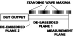
Fig. 6 Noise figure of a passive common-gate FET measured by the proposed method and calculated from its available gain.
As a conclusion to this section, the receiver calibration method proposed, using Equations 3 to 9, is suited for the extraction of transistor noise parameters, in particular when the noise parameter extraction method6 (F50 ) is applied, saving time (fewer power measurements are required - only from ON/OFF noise source states) and cost compared to tuner-based methods.
|
Table 1 | |||||
|
f |
NF |
sNF |
Gain |
sGain |
|NF-Gain| |
|
2 |
3.25 |
0.07 |
3.23 |
0.03 |
0.02 |
|
6 |
3.69 |
0.11 |
3.68 |
0.12 |
0.01 |
|
10 |
3.38 |
0.14 |
3.72 |
0.05 |
0.35 |
|
14 |
4.10 |
0.15 |
3.95 |
0.06 |
0.16 |
|
18 |
2.15 |
0.23 |
3.28 |
0.06 |
1.13 |
|
22 |
6.09 |
0.29 |
5.68 |
0.09 |
0.41 |
Using On-wafer Noise Sources for Receiver Calibration and FET Noise Parameter Determination
When using coaxial and waveguide noise-sources for measuring noise-parameters of microwave and millimeter-wave on-wafer FETs, the noise-source ENR, known from manufacturers' data, must be translated to the wafer-probe reference-plane through an input two-port adapter in order to calibrate the receiver. This step requires the determination of the adapter insertion loss (Gadapter ) from two calibrations performed with a network analyzer: two-port on-wafer (planes 1-1' and 2-2'); one-port (OSL) at the noise-source (coaxial or waveguide) port (plane 0-0'). The excess noise ratio (ENR') at the probe plane (plane 1-1') is determined from the known noise source ENR at plane 0-0' and the measured insertion loss of the input two-port adapter
At millimeter-wave frequencies, the OSL calibration uncertainty increases; therefore, the accuracy with which insertion loss and translated ENR are computed degrades. Furthermore, since the adapter insertion loss increases with frequency, the effective ENR at the wafer-probe plane is reduced to unpractical values. A solution to these problems is an on-wafer diode noise-source placed at the wafer-probe plane. Since there is no input adapter, the determination of diode ENR at the probe-tip does not require an OSL calibration, but only measured noise-powers and reflection coefficients GS , GR , determined from the on-wafer calibration.
Fig. 7 Noise diode wire-bonded to a Jmicro transition.
Two types of on-wafer noise sources have been considered and used here. First, a cold-FET (VDS = 0) with the gate reverse-biased. The device is a 0.5 mm gate-length, 2 x 50 mm gate-width DPD-SQW HEMT from the Foundry of Fraunhofer Institut, Freiburg, Germany (FhG-IAF). The gate bias point is fixed with a current source, close to the transistor breakdown point. This FET is used in a common-source configuration and its gate-source port is connected to the on-wafer reference-plane 2-2' as an inexpensive on-wafer diode. A commercial avalanche noise diode chip (Noise-Com NC-406) wire-bonded to the microstrip end (see Figure 7 ) of a coplanar-to-microstrip transition, Probe Point™ 1003 Adapter Substrate from Jmicro, is used as a hot source. To determine the equivalent noise-temperature Td of every noise device for a selected bias point, its noise power delivered to the receiver Pd and its reflection coefficient (GS HOT ) are measured. Combined with the measured noise power (PREF ) and the reflection coefficient (GREF ) of an on-wafer passive well-matched reference-load, the following expression is obtained for Td :
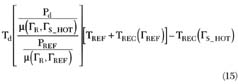
In Equation 15, TREC is the receiver noise-temperature evaluated for GREF and GS HOT , respectively, m is the mismatch coefficient defined in Equation 4 and GR is the receiver input reflection coefficient. To compute TREC, the receiver NPs previously determined from calibration with the coaxial noise source (Equations 7 to 9) are used. From Td computed in Equation 15, the diode ENR is readily obtained. To reduce the uncertainty in this measured on-wafer noise source ENR, equivalent circuit models for a cold-FET and an avalanche diode (including their intrinsic noise sources) are determined from the measured ENR and S-parameters (in the case of cold-FET) or reflection coefficient (in the case of avalanche diode), and their intrinsic noise current sources are fitted with frequency using their smooth frequency characteristic.9,10 Then, a final estimate of the ENR is computed from the model. Figure 8 shows the final estimate of the ENR and compares it to the measured ENR. Note that the ENR values obtained are high at the on-wafer plane 2-2', ranging from 8 to 20 dB with the cold-FET and from 20 to 34 dB with the avalanche diode, depending on frequency and bias point.
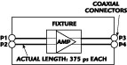
Fig. 8 On-wafer noise source ENR; (a) a cold-FET and (b) an avalanche noise diode.
Figure 9 compares the receiver NPs measured with a standard coaxial noise-source, to those measured with the on-wafer noise-sources whose ENR has been determined, using the receiver calibration method (Equations 3 to 9). The highly mismatched on-wafer noise-sources are used as the hot state, whereas a well-matched coplanar load at room temperature is used as cold state. A good agreement is obtained (agreement in the receiver Fmin measured with the avalanche diode is within the coaxial-source ENR uncertainty, ±0.34 dB at 40 GHz), demonstrating the applicability of the proposed calibration method to on-wafer noise sources.
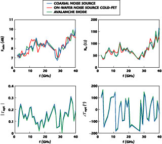
Fig. 9 Measured receiver noise parameter to 40 GHz.
Figure 10 shows an example of measured noise parameters of a PHEMT up to 40 GHz using the F50 technique6 and the receiver noise parameters, previously calibrated with both the cold-FET and avalanche diode noise sources. The FET noise-figure (F50 ) is obtained by using the above procedure (Equations 11 to 13). The results show very small differences by using either of the on-wafer noise sources.
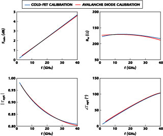
Fig. 10 Measured noise parameters of a PHEMT biased at Vds = 1.5 V, Ids = 17.9 mA.
Conclusion
A general method for calibrating the four receiver noise parameters using unrestricted noise sources, which does not require a tuner, has been presented. Specifically, this method allows very different hot/cold state impedances, simplifying the design of on-wafer noise sources (no lossy pad after the noise diode is required). The method makes some assumptions in the receiver. The influence of such assumptions in the receiver calibration and the determination of FET noise parameters (using the F50 method) are studied through a comparison with tuner-based methods. The receiver calibration is verified by measuring a mismatched passive device (common-gate FET). A reverse-biased cold-FET and an avalanche noise diode are used as mismatched on-wafer noise sources up to 40 GHz. The four receiver noise parameters are calibrated with the on-wafer noise sources and the receiver calibration method presented here, and applied to the measurement of an on-wafer HEMT noise parameter, using F50 .
Acknowledgment
This work has been supported by Spanish government grants 2FD97-0960-C05-05 and 2FD97-1769-C04-03 (CICYT-FEDER).
References
1. A. Lázaro, L. Pradell and J.M. O'Callaghan, "Method for Measuring Noise Parameters of Microwave Two-port," IEE Electronics Letters , Vol. 34, No. 12, 1998, pp. 1332-1333.
2. A. Lázaro and L. Pradell, "Extraction of Noise Parameters of Transistor Using a Spectrum Analyzer and 50 W Noise-figure Measurements Only," IEE Electronics Letters, Vol. 34, No. 24, 1998, pp. 2353-2354.
3. L.P. Dunleavy, J. Randa, D.K. Walker, R. Billinger and J. Rice, "Characterization and Applications of On-wafer Diode Noise," IEEE Transactions on Microwave Theory and Techniques , Vol. 46, No. 12, December 1998, pp. 2620-2627.
4. R.P. Hecken, "Analysis of Linear Noisy Two-ports Using Scattering Waves," IEEE Transactions on Microwave Theory and Techniques , Vol. 29, No. 12, October 1981, pp. 997-1004.
5. T. Werling, E. Bourdel, D. Pasquet and A. Boudiaf, "Determination of Wave Noise Sources Using Spectral Parametric Modeling," IEEE MTT-S International Microwave Symposium Digest , June 1997.
6. A. Lázaro, L. Pradell and J.M. O'Callaghan, "FET Noise Parameter Determination Using a Novel Technique Based on 50 W Noise-figure Measurements," IEEE Transactions on Microwave Theory and Techniques , Vol. 47, No. 3, March 1999, pp.315-324.
7. L. Escotte, R. Plana and J. Graffeuil, "Evaluation of Noise Parameters Extraction Methods," IEEE Transactions on Microwave Theory and Techniques , Vol. 41, No. 3, March 1993, pp. 382-387.
8. "Noise-figure Measurement Accuracy," Hewlett Packard Application Note57-2, November 1988.
9. M.C. Maya, A. Lázaro and L. Pradell, "Calibración del ENR de Fuentes de Ruido en Oblea," XV Symposium Nacional URSI , Zaragoza, Spain, September 2000, pp. 1-3.
10. R.H. Haitz and F.W. Voltmer, "Noise of a Self-sustaining Avalanche Discharge in Silicon: Studies at Microwave Frequencies," Journal of Applied Physics , Vol. 39, No. 6, 1968, pp. 3379-3384.
A. Lázaro received his MS and PhD degrees in telecommunication engineering from the Universitat Politècnica de Catalunya (UPC), Barcelona, Spain, in 1994 and 1998, respectively. He then joined the faculty at UPC, where he has been teaching a course on microwave circuits and antennas. His research interests are in microwave device modeling, on-wafer noise measurements, MMICs, low noise oscillators and MEMS.
M.C. Maya received her MSc degree in electronics and telecommunications from the CICESE Research Center, Ensenada, BC, Mexico, in 1998, and is currently working toward her PhD degree at the Universitat Politècnica de Catalunya (UPC), Barcelona, Spain. Her research interests are in MESFET, HEMT and HBT device modeling, and on-wafer noise measurements techniques.
L. Pradell received his telecommunication engineering degree from the Universitat Politècnica de Catalunya (UPC), Barcelona, Spain, in 1981. From 1981 to 1985, he worked at Mier Allende, S.A. (Barcelona) as an RF and microwave system design engineer. In 1985, he joined the faculty at UPC, where he received his PhD degree in 1989. Since 1985, he has been teaching courses on microwave circuits and antennas, and performing research on microwave and millimeter-wave devices and systems.
|
APPENDIX A
APPENDIX B
| ||||||||||||||||||||||||||||||||||||||||||||||||||||||||||||||||||||||||||||||||||||||||||||||||||||||||||||||||||||||||||||||||||||||||||||||||||||||||||||||||||||||||||||||||||||||||||||||||||||||||||||||||||||||||||||||||||||||||||||||||||||||||||||||||||||||||||||||||||||||||||||||||||||||||||||||||||||||||||||||||||||||||||||||||||||||||||||||||