
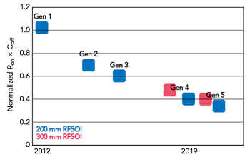
Figure 1 RF SOI small-signal figure of merit, Ron x Coff, vs. process generation.
The wireless data bandwidth needed to fulfill the promise of 5G imposes new performance requirements on the underlying specialty silicon technologies such as RF SOI and SiGe BiCMOS used in the front-ends of user equipment (UE), small cells and base stations. In this article, we review recent advancements in these platforms that support key 5G components like massive MIMO (mMIMO), the increased use of carrier aggregation, lower latency, beamforming and higher receive (Rx) sensitivity, all applicable to both the sub-6 GHz and mmWave spectrum.
Recently, Huawei’s chairman compared the fifth generation (5G) wireless technology to “the new electricity” when combined with other emergent technologies such as artificial intelligence. This is a remarkably bold prediction, yet not without merit. 5G is expected to connect the world truly as never before, with massive machine-to-machine, ultra-low latency and Gbps mobile broadband. With a smart mix of macro cells, small cells and localized user-premises systems, 5G will provide high speed, ultra-low latency and reliable connectivity. Entirely new industries and business models will develop, ones we can only imagine today, such as augmented and virtual reality, autonomous driving and remote medical care, including surgery.
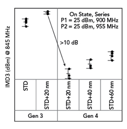
Figure 2 >10 dB reduction in RF switch IMD3 achieved from Gen 3 to Gen 4 of the 200 mm RF SOI process vs. gate length.
To monetize these opportunities, the race for 5G infrastructure deployment is well underway. China’s largest mobile service providers are aggressively rolling out 5G to 40 large cities using carrier frequencies in the sub-6 GHz regime. In South Korea, KT and other operators have enabled 5G in the country’s most populated areas. Verizon, AT&T and others are providing 5G service using a combination of traditional cellular and “mmWave” (really cm) wavelengths in selected U.S. cities. Deloitte estimated that 25 operators would launch 5G service in 2019, doubling to over 50 in 2020. Similarly, 20 handset vendors were expected to launch 5G ready handsets in 2019 and grow rapidly this year. The Global mobile Suppliers Association reported 78 suppliers had announced or released 208 5G devices through the end of January, including 62 phones. About 15 to 20 million handsets are expected to be 5G ready in 2020, increasing rapidly to 100 million in 2021. With a concurrent increase in RF content in 5G phones, the opportunity for the RF community is enormous, putting greater emphasis on system differentiation through IC design and semiconductor process innovation.
As a pure-play foundry focused on “more than Moore” technologies, such as specialty RF processes, Tower Semiconductor is enabling higher levels of performance for IC designers at top-tier front-end module (FEM) suppliers to support key 5G building blocks, such as mMIMO and carrier aggregation. In this article we provide an overview of recent advances in RF process technologies and design tools that underpin 5G base stations, small cells and UE.
INNOVATION for 5G SUB-6 GHz RADIOS
Using the additional spectrum becoming available at S- and C-Bands is one way service providers are increasing capacity. In the U.S., initial commercial deployment has been approved in the 3.5 GHz band. While the sub-6 GHz spectrum is familiar territory for UE FEMs, the increased data rates defined by 5G create opportunities and challenges for silicon RF technology.
RF SOI continues to be a workhorse for sub-6 GHz RF switching, as the key small-signal switching figure of merit Ron x Coff - the product of device on-state resistance and off-state capacitance, independent of device width - has dropped by more than 2x from first-generation SOI technology (see Figure 1). This improvement in small-signal performance translates directly to reduced power loss and better isolation, particularly for high throw-count switches, making it easier for FEM module suppliers to meet more stringent system requirements. It can also be leveraged to shrink the switch branches that typically dominate die area, reducing cost and saving FEM board space. 5G switch products that support mid-band frequencies are especially sensitive to Coff.
The increasing number of carrier aggregation combinations enabled by the latest 3GPP standards provides another challenge for FEM architectures. Intermodulation products generated by RF SOI switches during transmit (Tx) can cause de-sense problems on nearby Rx paths. Newer generations of SOI technology customized for RF switching show improved linearity (see Figure 2), which helps mitigate this issue. For digital integration, standard cells in thin film SOI require special consideration, owing to the lack of a shared body contact. The more advanced generations of RF SOI typically support higher digital densities that allow integration of mobile interface logic (MIPI) with reduced area and power consumption. The low latency requirements of 5G pushes switching times from the typical 5 μS to ~1 μS, which is challenging yet achievable in RF SOI with careful design.
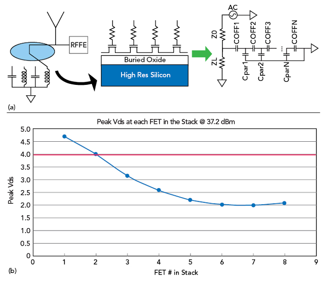
Figure 3 Stack of SOI FETs used for a high voltage antenna tuner is represented as a capacitive network (a) with a non-uniform voltage distribution across the FETs (b).
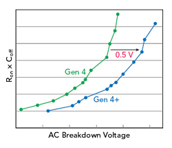
Figure 4 Generational improvement in Ron x Coff and peak RF breakdown voltage; each point represents a different FET gate length.
5G mMIMO is increasing the demand for antenna tuners based on aperture or impedance tuning. RF SOI is the incumbent technology for solutions that involve switching impedance elements or modifying the antenna effective electrical length. For this application, series stacks of I/O FETs are typically used to handle high VSWR near the UE antenna. Figure 3 shows a simplified schematic of the FET stack and the unequal voltage distribution resulting from substrate parasitics and other effects. These make it challenging to realize efficient FET stacks to handle >80 V in some tuner architectures. Specialized high power handling FETs with good small-signal figures of merit (Ron x Coff) facilitate antenna tuner designs (see Figure 4), since they make it easier to reach the voltage handling required of the stack. Process design kits (PDK) that enable these parasitic effects to be simulated with sufficient speed and accuracy enable the design of more sophisticated branches with lower insertion loss. Different assembly options (wire bonding versus flip-chip) can be simulated, as the packaging scheme significantly impacts the voltage distribution within the RF core. Where very high accuracy is needed, the designer can use electromagnetic (EM) simulation of the substrate and package and integrate the results with the PDK device SPICE models for circuit simulation.
RF MEMS, such as offered by Cavendish Kinetics (recently acquired by Qorvo), is a competing technology that offers superior small-signal performance, high voltage handling, wider tuning range and better linearity than SOI-based tuners. These characteristics will be more highly valued for 5G; however, time will tell if concerns about mechanical stability and reliability limit broad adoption of RF MEMS technology.