
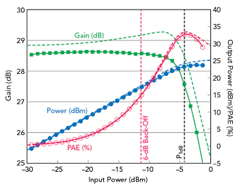
Figure 5 28 GHz PA gain, Pout and PAE.1
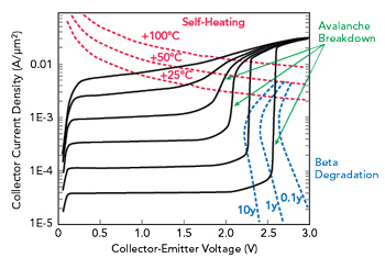
Figure 6 SiGe HBT I-V characteristics, showing the safe operating area for a PA design.
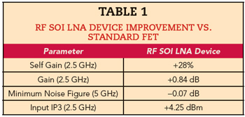
To improve the signal-to-noise ratio, another FEM trend is to move the main or diversity low-noise amplifier (LNA) closer to the UE antenna, where it can be combined with RF switching. On-chip impedance matching elements for the LNA can leverage the high resistivity SOI substrate for high Q-factors with this integration. Specialized LNA devices can now provide better self-gain and linearity than traditional NMOS (see Table 1). On the other hand, high performance SiGe HBT devices developed for much higher operating frequencies - ft and fmax >250 GHz - can offer better noise performance at lower supply current than MOSFETs. Tower Semiconductor offers low mask-count versions of high performance SiGe BiCMOS processes specifically tailored for stand-alone LNA applications. A slightly more complex process supports the addition of a customized RF switch with small-signal performance that rivals first-generation RF SOI. GaAs LNAs offer better dynamic range than SOI and SiGe but require higher supply voltages and draw currents that make them less suitable for battery sensitive mobile devices. The process technology choice for LNAs comes down to the application, architecture (i.e., LNA only or an LNA and switch), carrier frequency, power consumption and other FEM specifications.
Power amplifiers (PA) using GaAs HBTs have remained dominant in the UE for cellular Tx for 4G and are expected to remain so for 5G sub-6 GHz frequencies. Envelope tracking techniques should be more beneficial for 5G waveforms, given their higher peak-to-average power ratio. The more complex 5G modulation schemes motivate improvements in silicon platforms used for PA controllers: lower Rdson and higher digital density.
INNOVATION for 5G mmWave
A more integrated approach is generally required for the medium power Tx/Rx building blocks in the 28 to 40 GHz frequencies allocated in North America, Europe and Asia for 5G. Here, phased array architectures are needed to overcome the much higher path losses compared to the sub-6 GHz bands. For Tx, the choice is between using a fewer numbers of elements, each with higher output power provided by GaN or GaAs HEMT PAs, or using a larger array of lower power elements using RF SOI or CMOS PAs. Small (2 x 2 or 4 x 4) arrays of Tx/Rx chains can be arrayed to address a range of EIRP requirements. The technology of choice will depend on the required overall power levels. For small cells with up to 1 W per element, SiGe BiCMOS is in the sweet spot of power consumption and system cost.
For the PA at mmWave frequencies, SiGe HBTs offer better efficiency at high output power than FETs (see Figure 5). The figure shows the measured performance of a 28 GHz PA fabricated in SiGe BiCMOS, which delivers 21 dBm output power with 33 percent power-added efficiency (PAE) and 28 dB gain.1 SiGe BiCMOS phased arrays are already serving the Ku- and Ka-Band satellite communications market with high performance beamformers. Numerous publications from the University of California San Diego and other organizations have demonstrated the capability of this technology for phased arrays from 4- to 256-elements.2 With his architecture, uniform feed lengths and advanced SiGe BiCMOS processing ensure uniform performance across the elements, reducing or eliminating the need for costly calibration. For switching, one can use high speed HBT devices biased in reverse saturation.3 For successful PA design, the SPICE models should include self-heating effects and the device’s safe operating area (SOA), warning the designer of operating conditions outside the SOA during SPICE simulations (see Figure 6).
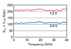
Figure 7 300 mm RFSOI Ron x Coff is flat from 1 to 40 GHz, shown for Vds = 1.2 and 2.5 V.
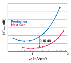
Figure 8 Noise figure at 5 GHz showing 0.15 dB reduction with next-generation process.
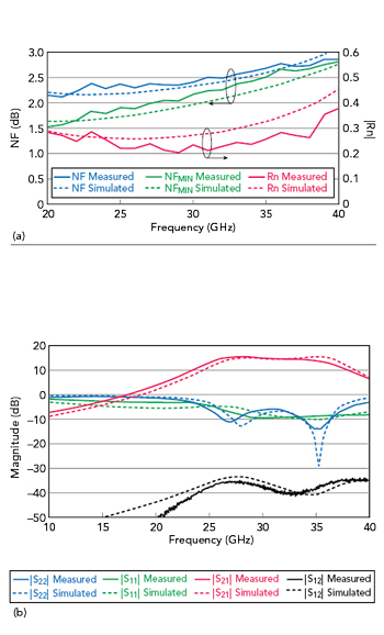
Figure 9 Measured vs. simulated noise figure, Rn (a) and S-parameters for a 26 to 35 GHz LNA fabricated with fifth-generation SiGe BiCMOS.
For the mmWave UE, lower power PAs in advanced CMOS or RF SOI become more practical, and SOI is still the best technology for integrating the Tx/Rx switches. The power handling requirements are relaxed compared to what is currently done at sub-6 GHz. Also, the Ron x Coff degrades little over the mmWave frequency range (see Figure 7). Since passive element area scales inversely with frequency, it becomes practical to consider including on-chip inductors to resonate out the capacitive loss from the off-state RF paths. Here again, the improved passive performance is an advantage afforded by RF SOI’s high resistivity substrate. Because available devices in advanced CMOS and SOI technologies lack the dynamic range of SiGe HBTs, the PA design is inherently more challenging. Self-heating in SOI PAs poses another technical challenge that must be mitigated through careful layout. GaAs HBT technology could be used as the final PA stage for better efficiency, albeit at higher cost. It will be interesting to see whether specialty RF technology such as SiGe or RF SOI can provide enough performance advantages for the mmWave Tx and Rx chain to win space in future FEM handsets, or whether this functionality will be integrated with the transceiver.
For the Rx path, the design can capitalize on the advantage of high speed SiGe HBT technology, which has evolved through many generations and is now providing >300 GHz ft and fmax NPNs in volume manufacturing with good yields. Designers can leverage the improved performance to run at lower power for 28 to 40 GHz applications. Lateral device scaling has reduced extrinsic base resistance in the more advanced processes, resulting in lower RF noise (see Figure 8). SOI is an alternative with good LNA performance and the ability to integrate passives and very good RF switches, as previously described. Foundry IP blocks and mmWave-friendly PDKs can significantly increase the probability of first-pass design success. Figure 9 plots the performance of a 26 to 38 GHz reference LNA fabricated with the Tower Semiconductor 180 nm SiGe BiCMOS process, showing good agreement between measured and simulated performance. Such designs are facilitated by accurate RF models in the mmWave regime, inductor and transmission line toolboxes and validated EM stack-up files. Figure 10 shows a 28 GHz LNA with on-chip matching and its measured and simulated small-signal performance. This design was fabricated with a 300 mm SOI platform with sub-100 nm gate lengths to achieve excellent noise figure. At these frequencies, the inductor Q is roughly 2x greater over the high resistivity SOI wafer than with a standard low resistivity Si substrate.
CONCLUSION
The 5G era is upon us, providing enormous market growth opportunities for the entire semiconductor ecosystem. The superior system performance required for Gbps speed, ultra-low latency and reliable 5G connectivity demands more stringent requirements on sub-6 GHz and mmWave radios. Specialty silicon process technology, such as SiGe BiCMOS and RF SOI, have evolved rapidly in the last few years to deliver the required performance for switching, LNA and PA applications in the price-sensitive, high volume consumer market. New capabilities have been added to the design environments of these platforms to minimize design cycles. Solutions for mmWave beamformers are manifold, and it is likely we will see different solutions adopted at different power levels, offering a range of cost versus performance choices.
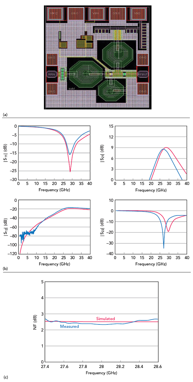
Figure 10 300 mm RFSOI LNA demonstrators (a) showing single-stage simulated (red) and measured (blue) S-parameters (b) and dual-stage design with 20 dB gain and 2.8 dB noise figure (c).
Acknowledgments
The authors thank the FEM R&D and manufacturing teams in Newport Beach, California; Migdal HaEmek, Israel; and Uozu, Japan.
References
- A. Sarkar, F. Aryanfar and B. A. Floyd, “A 28-GHz SiGe BiCMOS PA With 32% Efficiency and 23-dBm Output Power,” IEEE Journal of Solid-State Circuits, Vol. 52, No. 6, pp. 1680-1686, June 2017.
- S. Zihir, O.D. Gurbuz, A. Karroy, S. Raman, G.M. Rebeiz and V. Tech, (2015), “A 60 GHz Single-Chip 256-Element Wafer-Scale Phased Array with EIRP of 45 dBm Using Sub-Reticle Stitching,” Radio Frequency Integrated Circuits Symposium (RFIC), pp. 23–26.
- R. L. Schmid et al., “A 94 GHz 1.4 dB Insertion Loss Single-Pole Double-Throw Switch using Reverse-Saturated SiGe HBTs,” IEEE MWCL, Vol. 24, No. 1, pp. 56-58, January 2014.