

Responding to the market’s advance to mmWave frequencies for wireless and data rates approaching 100 Gbps for data communications, HUBER+SUHNER has developed a multicoax connector for circuit boards, enabling low reflection transitions from the cable assemblies to the PCB. Designed with the goal of achieving an electrically transparent connection, the MXPM70 provides performance through 70 GHz - optionally > 90 GHz - and is available in configurations including single and dual rows of eight coax cables with 2.54 mm center-to-center pitch. A magnetic locking mechanism maintains repeatable and precise connections between the socket and cables, ensuring consistent signal integrity. The gold-plated brass socket and aluminum connector housing were designed to be low-cost while achieving the stringent performance requirements.
BOARD TRANSITION DESIGN
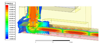
Figure 1 The transition, which converts the TEM wave in the coax cable to a planar wave propagating on the board, can introduce unwanted reflections if not properly designed.
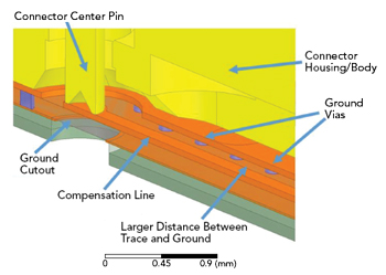
Figure 2 MXPM70 connector-to-board transition optimized for high frequency performance.
RF board connectors are challenging to specify, as their electrical performance depends on the design of the PCB footprint or transition to the interconnecting lines on the board. Selecting the best board connector requires understanding the design of the interface used by the connector manufacturer to determine the specified performance. Insertion loss, return loss and crosstalk are only valid for the same footprint and board configuration used by the manufacturer. Achieving this performance in the user’s application requires the same design or a new, carefully designed transition. Any changes in the dielectric material, substrate thickness and metallization thickness can have a significant impact on the actual performance of the user’s board. The transition, which converts the TEM mode of the coaxial cable to a planar mode propagating on the board, is the most sensitive part of the design, potentially creating reflections with attendant suck-outs in insertion loss, particularly near the upper end of the operating frequency range (see Figure 1).
To achieve the specified performance using the MXPM70 board connector, HUBER+SUHNER recommends using electromagnetic (EM) simulation to optimize the user’s board footprint for the connector. Begin by choosing the transmission media on the board - typically microstrip, stripline or grounded coplanar waveguide (GCPW) - and the board structure, i.e., board material and thickness, number of layers, metallization and thickness. Design an initial layout of the footprint, analyze the performance of the interface and iterate the layout to optimize performance. To illustrate, the design of a transition to GCPW using the board stack-up of Table 1 was optimized, resulting in the footprint shown in Figure 2.
To minimize parasitic capacitance, a ground cutout was incorporated on layer L2 under the signal pad on layer L1, since the size of the signal pad cannot be reduced. The minimum size of the signal pad is set by the connector center pin and positioning tolerances to ensure electrical stability and mechanical robustness. While the cutout increases losses slightly at lower frequencies, it improves the high frequency performance significantly and has minimal effect on the crosstalk between connectors. One caution: the ground cutout should be evaluated to ensure it does not allow parallel modes within the stack. A second design choice to minimize the parasitic capacitance was extending the distance between the signal line and its ground on L1.
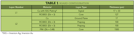
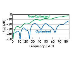
Figure 3 Simulated |S11| of the MXPM70-to-board transition.
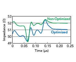
Figure 4 Simulated time domain response of the MXPM70-to-board transition.
To improve impedance matching and signal transfer to the GCPW transmission line, a compensation line was added to L1. PCB traces are commonly designed with impedances of 46 to 48 Ω to minimize losses and compensate for the etching process during manufacturing. Etching reduces the transmission line width, increasing the impedance - which can cause mismatch with connectors designed for 50 Ω. The compensation line provides a gradual impedance transition, yielding lower insertion loss and minimizing capacitive effects.
EM modeling this design shows |S11| better than −15 dB through 80 GHz (see Figure 3). Simulating the time domain response of the transition shows the impedance is between approximately 49.5 and 52.5 Ω (see Figure 4). To show the performance improvement achieved by optimizing the footprint, the |S11| and time domain responses are also plotted for the non-optimized board design.
SUMMARY
While a generic footprint design can be used during the early phase of development, to place the connectors and route the RF or data channels on the board, the footprint must be optimized for the specific board configuration to achieve the highest frequency and data rates. While the footprint design may seem straightforward, not analyzing and optimizing the transition can significantly degrade test results and the overall performance of a high cost system.
With appropriate board design, HUBER+SUHNER’s MXPM70 multicoax connector is well suited for RF and high speed data applications, providing low reflection coax-to-board transitions with performance to at least 70 GHz - pretty close to electrically transparent.
HUBER+SUHNER AG
Herisau, Switzerland
www.hubersuhner.com