

Can you tell us the roots of the company and how it was formed?
Benchmark’s Lark RF Technology has been serving aerospace, defense, telecom and industrial customers for 33 years. In 2015 Lark RF was acquired by Benchmark, which has 42 years of experience of its own supporting regulated industries. We’ve expanded our U.S. operations beyond our 55,000 sq. ft. design and manufacturing center in Tijuana and moved our office from Anaheim to Phoenix to coincide with Benchmark’s move to Arizona. We have 20,000 sq. ft. under one roof in Phoenix, and nearly 300 employees.
What unique technologies and processes does Lark offer to the high frequency market?
Lark’s next generation circuit design and fabrication was built around solving RF and high speed challenges with capabilities above 10 GHz. We have expertise in a number of processes and substrates, but we are really the leader in advanced liquid crystal polymer (LCP) manufacturing methods. LCP is thin, flexible and has superior power handling ability with roughly half the loss of typical polyimides, making it a great choice for a high density interconnect (HDI) board material.
We have the ability to design and fabricate our own circuits with parts, material and processes optimized for design at 10 GHz and beyond. We coupled that with our vertically integrated design team, SMT and advanced micro-electronics, to create a one-of-a-kind capability to simplify our customers’ design process and accelerate time to market. It’s not just that we have better tech, we have also made it so much faster and easier to get through the engineering phase of product development and into production.
Can you tell us about your RF and High Speed Design Center of Innovation in Phoenix and what is unique about it?
Benchmark has re-imagined the whole foundation of electronic circuits at the RF and High Speed Design Center of Innovation in Phoenix. We have invested in state-of-the-art technology and equipment to create high aspect ratio circuits, plus we offer a unique set of design and manufacturing capabilities with low loss substrate base materials, such as LCP. Both RF and digital applications are concerned with loss. Loss translates into wasted power for the customer, and that lost power generates heat. One of our core competencies is to help minimize loss to improve thermal management and overall system efficiency, so we have a broad range of tools to address that in the Innovation Design Center.
The company offers an interesting liquid crystal polymer packaging process; can you tell us about the advantages of that material and process?
The advantages are that it is superior in performance and design flexibility in high speed data and microwave applications. LCP provides a basic design platform to allow existing designs to scale into next generation telecommunications and broadband without changing all of the components or the overall design. It also has miniaturization applications in medical and industrial applications, including connected devices and overall reduction of size, weight and power (SWaP) in aerospace and defense.
Lark is able to reduce the size of traditional circuits by about 60%, how are you able to accomplish that (please provide an example or two with images)?
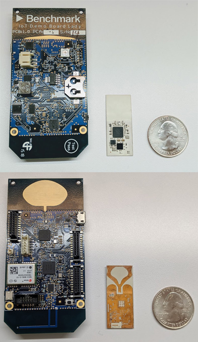 We have a number of tools at our disposal within our design approach. First and foremost, we drive adoption to high density interconnect (HDI) topologies to improve design efficiency. Additionally we have mastered the implementation of ultra-fine line and spacing, allowing us to achieve 1 mil lines and spaces reliably in production applications. By having our circuit design and fabrication vertically integrated and collocated with microelectronics, we have the ability to remove superfluous packaging in order to create hybrid designs. Using just one of these methods typically achieves nominally 60% improvement, although that can be even higher for customers who haven’t yet used any of these methods on their designs and redesign using multiple strategies.
One example of this is a MicroRadio, which is basically a miniaturized highly-precise IoT asset tracking tag. It has an accelerometer, a Nordic microcontroller and an ultra-wide band transceiver module. The MicroRadio is 1.2” x 0.7” x 0.56”, whereas the original conventional design was 3.5” x 1.75” x .056”. We were able to do this using our capabilities to manufacture less than 1 mil lines and spaces in substrate boards, as well as placing vias in the pads and using embedded traces.
How does Lark address thermal and mechanical requirements in high frequency designs?
First, miniaturization, adopting HDI principles and using dialectics that are optimized for the given application will drive overall system efficiency, while reducing loss and thermal profile of the system. Our tools allow us to balance thermal performance against design needs. We also have tools like low-density cores and copper planes in HDI topologies to efficiently remove heat.
What other methods do you use to address SWaP reduction?
The next level goes above the circuit interconnect design to the assembly design. Traditionally, designs are partitioned and use cabling, connectors and flexible interconnect. Because of our unique technology we are able to re-think how systems are partitioned in order to create heterogeneous designs that will mix RF, digital, power and control, and in doing so, will eliminate the need for multiple partition boards. This simplifies bills of material by removing flexible interconnect and connectors to reduce cost, while also simultaneously reducing SWaP. In our model, essentially, three boards become one.
What advantages do you offer in the 5G and IoT markets compared to other companies?
Scalability of design into NextGen 5G is the biggest advantage we offer. Our materials will naturally scale and be functional with various chipsets, so you won’t need to redesign as you need to change to a new connectivity type. You don’t have to redesign the whole device if you need a different frequency range in the future.
Can you tell us about your solutions and services for Aerospace and Defense markets?
Since our skill set applies to nearly everything in electronics, we do the hard things first. We are engaged in advanced research and development with a number of large U.S. aerospace and defense companies as well as RF design and fabrication for telecom satellite applications and other payload applications on low-Earth orbit satellites. We are supporting design and development of NextGen radars, sensors and radios at millimeter wave frequencies.
What are your future plans for new solutions and services?
Ultimately we’re not a product company, we align our investment in parts, material and processes together with our customers’ to ensure we have the capabilities to enable our customer’s roadmaps.