
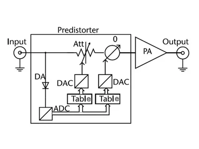
The main role of a microwave amplifier is to increase the level of an input signal (e.g. an oscillation span, amplitude, or power) without introducing noticeable distortion in the signal waveform, its spectral composition and the ratio of a signal to noise at the input. Any processing of a signal introduces unwanted distortion of some level. With signal amplification there is frequency distortion, nonlinear distortion, and interference. In linear circuits, frequency distortion is caused by signal transformations in which reactive parameters are not dependent on signal amplitude. Non-linear manifestations are varied. Among them are intermodulation distortion caused by the interaction of spectral components of one modulated signal and cross distortions are caused by the interaction of modulation components from several signals within a frequency bandwidth. Interference, which appears at the amplifier output, can be additive (instantaneous values of interference summed with instantaneous values of the signal) or multiplicative.
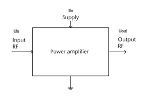
Figure 1. Diagram of an amplifier stage.
uin1 (t) = U1sin(2pf1t) or
uin2 (t) U1[cos(2 pf1t) + cos(2 pf2t)] (1)
The value of U1 can be found using the input power Pin with a known input impedance Rin as
U1 = (2PinRin)1/2 (2)
By default, one can assume Rin = 50 ohms.
We can also assume that the amplifying active element is nonlinear and inertia-free; it creates an output with frequencies +mf1 +nf2 (coefficients m and n are arbitrary integers). The amplitudes of these spectral components depend only upon the amplitude of the input signals and the coefficients of nonlinear conversion. Components of the third order with frequencies 2f1- f2 and 2f2-f1 appear in the spectrum structure of the output signal near frequencies f1 and f2. The power of these intermodulation components is proportional to U1 3 (see Figure 2).
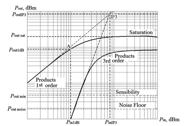
Figure 2. Amplitude characteristics of double-tone signal intermodulation products.
While the power of the output spectral components of the first order with frequencies f1 and f2 increase with input power at a 10 dB/decade slope (i.e. linearly), the components of the third order increase at a 30 dB/decade slope. In the absence of saturation (i.e. by extrapolating their log linear small signal input/output relationships), powers of the first and third order products are equal at the third order intercept point (IP3). The value of PinIP3, or equivalently PoutIP3, characterizes the level of an amplifier’s nonlinear distortion. At increased values of Pin, saturation limits the Pout/Pin dependence in a transistor amplifier. In microwave tube amplifiers (e.g. travelling wave tubes (TWT) and klystrons), when Pin exceeds Pin sat, Pout decreases.
The value Pin1dB, and equivalently Pout1dB, at which compression at the output does not exceed 1 dB, is widely considered to be a conditional boundary for maximum signal level in a linear mode. The level of background power of the amplifier’s inherent noise reduced to the input (i.e. the noise floor) defines the lower boundary of the amplifiers dynamic range.
Efficiency of a power amplifier η = Pout/Pdc is the ratio of microwave output power Pout to power consumed by the DC power supply. For transistor amplifiers with insufficiently high gain, G = Pout/Pin, it is more accurate to use power added efficiency PAE = (Pout - Pin)/Pdc, which subtracts the power contributed by the preceding stage(s). The relationship between these measures can be expressed by:
PAE = η (1-1/G) (3)
To characterize the mode of an RF transistor power amplifier (PA), one can use the designation of classes from A to F. We introduce the current conduction angle q in the input circuit, which is the normalized characteristic of the input signal amplitude U with respect to the difference between the current cutoff DC voltage E’ and the bias voltage Ebias.
cos q ~ -(Ebias – E’)/U (4)
Class A (see Figure 3) corresponds to small signal operation in the linear region of the transistor’s input characteristics. Class AB corresponds to operation with a cutoff angle from 180 to 90 degrees, Class B corresponds to operation with a cutoff angle near 90 degrees, and the Class C mode corresponds to operation with cutoff angle from 90 to 0 degrees.
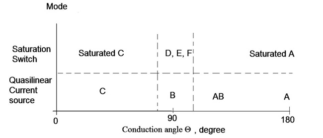
Figure 3. Transistor amplifier classes.
Switching modes of radio frequency amplifiers enable PAE increases up to 70 to 90 percent, but for comparatively low frequencies up to 1 GHz. Quasi linear Class C operation for high frequency PAs also enables a PAE increase; however, its compression characteristic is non-monotonous (see Figure 4).
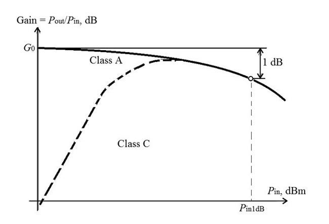
Figure 4. Class A and C amplification compression characteristics.
Classification and Parameters
There are many varieties of amplifiers for RF and microwave applications. Figure 5 illustrates one way of classifying them. There are several key elements, which include the operating frequency band, small-signal gain G0, maximum output power Pout max, active element technology, the design solution and the level of nonlinear transformation products. Amplifiers may be designed and optimized for power or efficiency. Cascaded amplifiers have similar values of input and output impedance (typically 50 ohms) and are connected in series so that the total gain expressed in decibels is equal to the sum of the individual stage gains. In gain control amplifiers (GCA; some manufacturers use the abbreviation VGA-variable gain amplifier) gain is changed by an external analog or digital signal. High linearity amplifiers have wide linear dynamic ranges, while limiting amplifiers are designed to saturate in order to reduce spurious variation of the input signal power.
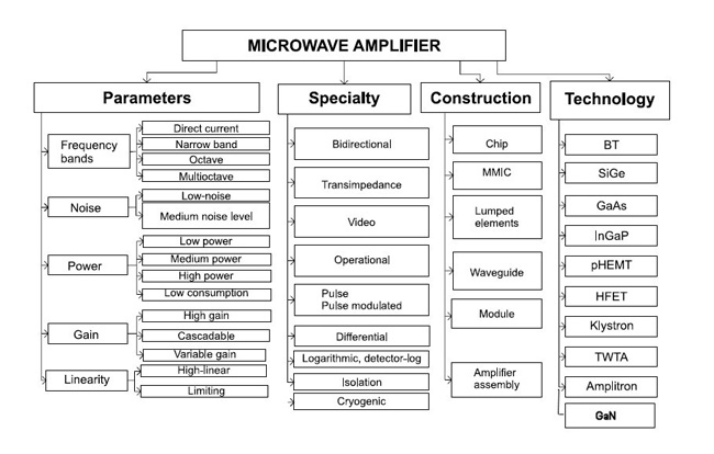
Figure 5. Radio frequency amplifier classifications.
When evaluating maximum output power of an amplifier, one must take into consideration its operating frequency. Device geometric dimensions decrease with increased operating frequency. Surface and volumetric energy density grows, introducing heat dissipation limitations. The level of amplifier output power is thus inversely proportional to the square of the operating frequency for a given device technology and thermal design. The summation of power from several active elements allows growth of the output power level but complexities arise with construction, energy efficiency of power splitters and combiners, phase synchronism of summed channels and prevention of spurious self-excitation. Because of these factors, for the decimeter wavelength range (frequencies up to 3 GHz), the conditional boundary of the high power stages is 100 W, for a portion of the centimeter range (frequencies up to 30 GHz) it is 10W, and for frequencies above 50 GHz more than 1W may be considered a high power.
A bidirectional amplifier amplifies the power of a source signal to be transmitted by an antenna transmitter signal, while a signal received by the antenna through the same connections passes to a low-noise amplifier and then to a receiver.
A transimpedance amplifier converts an input current into a voltage. It is used, for example, to match the output impedance of an RF input to a fiber-optical communication line with the input impedance of a laser diode or the output impedance of photodetector with the input impedance of a microwave section.
Special-purpose amplifiers are designed for specific communications standards (e. g. GPS, IEEE 802.11, WiFi, WLAN, 64QAM). Front ends include low-noise preamplifiers in combination with the frequency downconverters prior to baseband processing.
The logarithmic (log) and antilogarithmic (antilog) amplifier, variants of operational amplifiers (op-amp), are nonlinear circuits, in which output voltages are proportional to the logarithm (or exponent) of input voltages. Such amplifiers are used in intermediate frequency sections for compression (or extension) of the input power dynamic range, or for automatic gain control. For a logarithmic amplifier, the input signal amplitude interval (from Vin,min to Vin,max) is transformed at the output to:
Vout = -K ln [Vin/Vref] (5)
where K is a constant coefficient and Vref is a reference voltage.
The technology for the active element defines power supply parameters and the amplifier application. For solid-state amplifiers, besides silicon bipolar transistors (BT), new technologies have been developed around materials and structures such as SiGe, GaAs, GaN, InGaP, LDMOS, pHEMT, AlGaAs/GaAs, HFET, and pHEMT.
To provide high and ultrahigh output power in the microwave range, power amplifier tubes, such as klystron amplifiers, and traveling-wave tube amplifiers (TWTA) with different variants of slow wave structures are used.
Consider the following parameters:
- Operating frequency range with boundaries flow and fhigh.
- Small-signal gain G0 = Pout/Pin; voltage gain GVO = Vout/Vin, or small-signal power gain GPO = Pout/Pin; when using the logarithmic scale numerical values of GVO = 20log10 (Vout/Vin) in dB and GPO = 10log10 (Pout/Pin) dB in dB for the same input and output impedances.
- Noise figure (NF).
- Maximum output power of a linear amplifier Pout1dB.
- Maximum output power in saturation Pout sat.
There are no generally accepted low flow and high fhigh boundaries for an amplifier’s operating frequency band. One may specify by default such frequency values as cutoff frequencies at which the gain G0 decreases by 3 dB compared to the value in the middle of the operating frequency band. The absolute frequency bandwidth (BW) = fhigh–flow defines the range over which distortion of input signals is within an acceptable range for an application. The relative frequency BW kf = 2(fhigh–flow)/(fhigh+flow): for narrowband amplifiers kf << 1; for octave amplifiers kf ~ 2 and for multi-octave amplifiers kf > 2. For some models one may specify direct current (DC) as a lower bandwidth boundary so that in this case the kf value loses its sense. In these cases the value of the low cutoff frequency flow is defined by the frequency properties of bias circuits and blocking elements.
For wideband amplifiers the maximum gain flatness in the operating frequency band is specified. In some applications (for instance, for compensation of the frequency dependence of the other elements in a chain) amplifiers are designed with a given (positive or negative) slope value Sf = dG0/df for the amplitude-frequency characteristic in the operating frequency band.
For amplification of a bandpass signal there may be distortion caused by deviation from a linear phase characteristic: the function f(f) of the phase shift f = fout – fin in the amplifier with respect to a carrier frequency. As the quantitative characteristic of this phenomena we can use the non-uniformity of the signal group delay tgr = | df/df | in the operating frequency band.
An amplifier’s noise properties are defined by its noise factor Fnoise, which indicates how much the power spectral density (PSD) of the amplifier’s inherent noise exceeds the PSD of a resistor with resistance equaled to the input stage resistance. The noise temperature in Kelvin
Tnoise = T0 (Fnoise – 1) (6)
is called the amplifier noise temperature, where T0 = 290 K is standard (room) temperature. As a noise amplifier characteristic one most often uses the noise figure (NF) expressed in decibels
NF (decibels) = 10log10Fnoise (7)
For amplifiers dedicated to processing sinusoidal reference signals, we may specify values power spectral density (PSD) of the amplifier phase noise Sj(F) at different frequency offsets F near the carrier frequency, which increases the total level of a system’s output signal phase noise. Typical values at 10 GHz are -145 dBc/Hz at an offset of 100 Hz from the amplified signal with a white noise noise level of 170 dBc/Hz at an offset of 1 MHz and beyond.
PinIP3 is used for quantitative estimation of amplifier nonlinear properties (i.e. intermodulation distortion (IMD)). Alternatively PoutIP3 may be specified. The OIP3 value is expressed in dBm, it exceeds the Pout1dB value, and corresponds to an inadmissible level of distortion. For high power microwave amplifiers it is necessary to take into account amplification compression characteristics (AM/AM compression) and amplitude-phase conversion characteristics (AM/ PM conversion).
Sensitivity in a receiver is normally taken as the minimum input signal (Pin min) required to produce a specified output signal having a specified signal-to-noise (S/N) ratio. Dynamic range of an input signal level for a linear amplifier is the following ratio expressed in decibels:
D = 10 log (Pin 1 dB/Pin min) (8)
In a linear mode, an amplifier’s frequency-dependent complex S-parameters can be measured. One may also use X-parameters of power amplifiers, which are a generalization of S-parameters, taking into account the amplitudes of input and output signals.
Sensitivity of gain to supply voltage variations can be characterized by a variation of G0 in decibels per volt of supply voltage and sensitivity to environment temperature variations by variation of G0 in decibels per degrees Celsius.
The following additional characteristics are also important: weight; dimensions; mounting arrangement; input, output and bias connections; rated impedance of input and output circuits; and sensitivity to the environment: vibration, shock, moisture, radiation level, and static electrical and magnetic fields.