RF, microwave and millimeter-wave switches and switching matrices provide a variety of important functions, including:
- Control of frequency, power, various circuit parameters, and circuit configurations
- Modulation of signal phase, amplitude, and frequency
- Antenna duplexing for reception and transmission
- Switching to backup (automatic switchable redundancy) units and channels of data transmission
- Control of the beamforming, scan direction, and other parameters of antenna arrays
- Connection of test signals and measuring equipment for the fulfillment of automated measurements
- Digital control of sources, phase shifters, attenuators, delay lines
- Connection of an input port variety to an arbitrary port from a variety of output ports.
Applications differ, for example, by the level of power, frequency, required switching speed, quantity and configuration of simultaneously switched circuits, external environment, control signals, and packages. Therefore, the assortment of the switching components and technology is manifold.
Fundamentals
In the microwave region, switch development requires the consideration of signal parameters (e.g power, amplitude, phase, noise) in input and output lines or ports, which influence the functioning of adjacent units in ON and OFF states (see Figure 1).
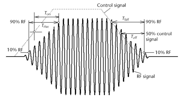
Figure 1. Switching speed parameters.
These parameters change during the switching process from the ON to the OFF state and vice versa. The rise time Trise is the time it takes for the RF signal to rise from 10 percent to 90 percent of the ON level. The fall time Tfall is the time it takes for the RF signal to fall from 90 percent to 10 percent of the ON level. The ON time Ton is the time interval from 50 percent of the control pulse to 90 percent of the ON level. The OFF time Toff is the time interval from 50 percent of the control pulse to 10 percent of the ON level. An ideal switch would have zero Ton and Toff (i.e zero delay and zero rise and fall times) with no accompanying transient oscillation or distortion of the incoming signal, except to gate it on or off at the output.
The transient interval between ON and OFF states may have a non-ideal oscillating character depending on the switching technology and switch construction. In a mechanical relay switch, for example, the position in time of the output signal edge may be delayed in a damped oscillatory manner relative to the edge position of the control signal. This has three contributors: 1) an inductive delay in the coil, 2) the time it takes for the physical movement of its contacts, and 3) the bounce time of the RF contacts.
Additional interfering phenomena can occur for even the simplest microwave single pole single throw (SPST) switch. This is attributed to the response of the input or output on frequency dependent RF reflection, lack of coincidence between the switching moment and oscillation phase, the occurrence of higher order transmission line modes, the dependence of circuit S-parameters upon incident power levels, the oscillating character of transients, and nonlinear transformations of the input signal within the switch.
More complex switches differ by the number of ports and positions. One can describe them in terms of multiport networks for multiposition and matrix switches, i.e.:
[B] = [S][A] (1)
where [B] and [A] are matrices of the output and input circuit, accordingly, and [S] is the scattering (transfer) matrix of dimensions m x n, where m is the number of input ports and n is the number of output ports.
The formula (1) represents an idealized model of a sinusoidal signal passage through a linear circuit with known parameters of waves that are incident upon ports and reflected from them. The matrix coefficients in (1) at each signal frequency are defined by the configuration, dimensions, and internal structure of the switch. Equivalent circuits are typically provided by a manufacturer for performance modeling. This equivalent circuit should satisfactorily describe behavior for frequencies exceeding several times the operating frequency in order to evaluate the impact of higher harmonic signals on the signal spectrum.
For a switch with ohmic contacts, the lower frequency boundary of its bandwidth in an ON condition is direct current (DC). Capacitive switches do not pass the direct current. The upper boundary in an ON condition is defined by spurious circuit parameters introducing transmission losses. In an OFF condition, the upper boundary is defined by spurious capacitance or poor isolation that allows the passing of unwanted signals between the input and output circuits, as well as ohmic losses.
Most switch architectures are reciprocal, their forward and reverse transfer characteristics are identical; however, some models of switches, for example, use ferrite or embedded amplifiers (i. e. nonreciprocal elements) so that the input and output ports cannot be changed.
Simultaneous switching of several input and output ports in a large matrix of switches requires determination of the variety of initial and resulting states and paths. To reduce the number of given combinations, custom software is often used.
The variation of each port’s matching conditions in the ON and OFF states, as well as during transition, is important because it may lead to inadequate circuit performance. In this regard, switching circuits can be complicated in order to minimize the impact from switching transients and to ensure the connection of matched loads to open ports.
Switches have limited power handling capabilities and service life depending upon the switching principle, manufacturing technology and materials, as well as the application. Switching in the absence of incident RF (i.e. “cold” switching), for example, induces less stress for higher reliability and a more prolonged life cycle, while increasing switched current decreases reliability and service life.
Classification and Parameters
RF, microwave, and millimeter-wave switches possess various combinations of properties, configurations and constructions. One can distinguish two-position, multi-position, and matrix switches according to the switching configuration. Variants are shown in Figure 2. The basic function is the connection and disconnection of contacts in a circuit through which high-frequency current flows.
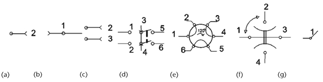
Figure 2. Switch configurations: SPST (a), DPST (b), SPDT (c), DPDT (d); Rotary Transfer 3x120 [1-2; 3-4; 5-6 or 2-3; 4-5; 1-6] (e), Rotary 3-position switch [1-3 or 1-4; 2-3 or 2-4] (f), and SP4T (g).
The simplest mechanical single pole single throw (SPST) switch has two terminals, which can be connected or disconnected (see Figure 2a). With two terminals for the coil, such as a relay there are four terminals in total. The pole may be normally-open or normally-closed when the relay is not energized. Adding another output makes it a single pole double throw (SPDT); one output is ON while the other is OFF (see Figure 2b). This can be extended to an arbitrary number of output ports (i.e. SPNT), where one port is on while the others are off. A double pole double pole double throw (DPDT) switch has two pairs of terminals (ports), equivalent to two SPST switches or relays actuated by a single coil (see Figure 2c). The rotary transfer switch is a variant of the two-position switch with the rotor capable of rotational orientation in one of two orthogonal positions as shown in Figure 2d. In the first position of the rotor the terminals (ports) 1 and 2 and 3 and 4 are connected; in the second position, 2 and 3 and 1 and 4 are connected. This circuit can be used to insert or bypass an amplifier, to change an antenna connection between transmission and reception (Tx/Rx), or to connect two microwave transmitters to two alternative antennas. A similar circuit with three contacts spaced +120 degrees apart (see Figure 2e) is suitable for waveguide realization. To increase the number N of switch positions for SPNT switches one can combine simpler circuits (see Figure 3).
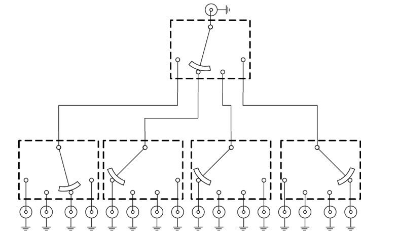
Figure 3. Electrical block diagram of a SP16T fan-out switch.
Switches may be implemented by means such as electromechanical (including reed) relays, solid-state relays, micro electromechanical systems (MEMS), non-reciprocal (e.g. ferrites), as well as manually and through programmable circuits. A relay is an electrically operated switch. Relays are used where it is necessary to control a high power circuit with a low power signal. In electromechanical relays, connection/disconnection is enabled with electromagnets and a mechanical mechanism external to the RF circuit. Vacuum-sealed contacts, which connect/disconnect with the help of the external magnetic-static field, are similarly used in reed relays; here the switching mechanism and the RF conductor are the same. In solid state relays, electrical resistance between input and the output ports is employed. It can be achieved by changing the bias voltage in a semiconductor consistent with the specific technology (e.g. PIN diode, GaAs FET) and the specific circuit structure connection (absorptive, reflective). In MEMS switches a microscopic mechanical electrically conductive strip is formed on the surface of a chip, with one end suspended above a contact. This mechanical actuator moves under influence of controlled electrostatic forces to connect the input and output circuits. Typically, nonreciprocal ferrite switches are those in which the magnetic field direction is changed. Switches with the manual control are typically used in measuring and calibration sets. For a programmable switch, its state is controlled by coded signals from a digital control unit.
Failsafe is a mode of operation in which the switch moves to the closed position when the actuating voltage is applied and always returns to a predetermined position when the voltage is removed. This is typically realized by a return spring within the drive mechanism.
A latching relay has two relaxed (bistable) states. The switch remains in a preselected position whenever the actuating voltage is removed or interrupted, and holds that preselected position until a voltage is applied to move it to another position. This can be accomplished with either a magnetic or mechanical latching mechanism.
Normally open (NO) or “push-to-make” is a mode of operation in which all output ports of the switch are disconnected from the input port until a voltage is applied to maintain a selected position. The switch returns to its open position with voltage removal. A polarized relay remains in the last stable position after disconnecting the control signal. Normally closed (NC) or “push-to-break” can be distinguished according to the state of the circuit. A switch with both types of contacts is called a changeover switch.
Terminated or non-terminated switch modes differ according to the loading of the open circuit. A terminated switch contains in its construction an internally matched load in each output port that ensures a low value of VSWR in both the OFF and ON states (i.e. the port in the ON state is matched to the connecting circuit, while the ports in the OFF state are matched to internal loads).
A self-cutoff option disables the actuator current after actuation. Either a series contact (linked to the actuator) or an IC driver circuit enables the cutoff. This option minimizes power consumption. Pulse latching is a term sometimes used to describe a switch without this feature.
A blocking matrix switch has switches on both the inputs and outputs. Therefore, each input signal can be switched to one individual output port. An example of an application for a blocking switch matrix is a radio and antenna system where each radio is connected to a unique antenna. If an application requires an input to be available to more than one output simultaneously, then a non-blocking matrix is used. Non-blocking switch matrices are used in applications such as multiple- input multiple-output (MIMO) transceivers and satellite station receivers.
Full fan-in and/or full fan-out matrices are characterized by the complete set of connection variants with up-stream and down-stream ports. Inter-channel crosstalk for matrices is a measure of the high-frequency signal leakage from one channel to another. It is the result of stray capacitance, mutual inductance, and leakage resistance between channels.
Low-power, medium-power, and high-power switches are distinguished according to the level of switched power.
An indicator tells the system, at which position the switch is in. Indicators are usually a set of internally mounted DC contacts linked to the actuator.
Parameters
The following are some important performance parameters:
- Operating frequency band, typically defined by boundary values of the input frequency for which the loss in the ON state increases by 3 dB; insertion loss (IL) in the ON state is expresses in decibels.
- Voltage standing wave ratio (VSWR) in each state.
- Isolation of the OFF circuit (in decibels) is the ratio of signal level at the input divided by the output signal level. Isolation, in dB, is a positive number.
- Power handling of the input signal Pmax. By default Pmax is the level of input signal power at which signal loss in the ON state increases by 1 dB. In microwave contact switches the maximal power handling of the input signal may arise due to arcing, and contact heating. In solid-state switches, switching power limitations are related to impedance variations in the active zone of the semiconductor material dependant upon the instantaneous voltage (the sum of the bias and high-frequency voltages). Nonlinear distortion of the passing signal may increase with increasing input power. One reason for limited power handling in RF switches, amplifiers, and waveguides in space applications is the multipactor effect, or secondary electron emission, which can cause device failure.
- Life cycle of microwave switches is defined principally by the technology and functional arrangement of the switching zone. In electromechanical switches, for example, contact wear-resistance may depends on whether switching is provided at low input RF power levels (cold) or at the high power levels (hot). Solid state switches have much longer life cycles without the noticeable degradation of key parameters.
- Signal group delay.
- Type, level and polarity of control signals, e.g. transistor-transistor logic (TTL), emitter-coupled logic (ECL).
- Operating temperature, typically -40° to +85° C.
- Passive intermodulation (PIM) or passive intermodulation distortion is the unwanted amplitude modulation of signals containing two or more different frequencies in a system with nonlinearites. A PIM product is the result of at least two multiple high power tones mixing induced by ferromagnetic materials, junctions of dissimilar metals, metal-oxide junctions, contaminated junctions and loose connectors. A typical input power level for testing passive devices is +43 dBm and if the permitted PIM is -120 dBm, the resulting PIM level is -163 dBc. Common third-order intermodulation is -110 dBc and a low level is -160 dBc.
The general specification and testing methods for switches and matrices are defined in MIL-DTL-55041.
Solid-State Switches and Matrices
A solid-state switch provides the functionality of an electromechanical relay but has no moving components, increasing long-term reliability. Solid-state switches also leverage large-scale semiconductor assembly and automation capabilities for lower cost; and, they occupy smaller footprints (transistors are on microscopic levels), which helps in the design of compact systems.
The characteristics of solid-state switches depend largely on the type of the switching semiconductor element, e.g. positive-intrinsic-negative (PIN) diodes, gallium arsenide GaAs or gallium nitride GaN transistor technology and Schottky diodes.
The maximum frequency fmax of the switched signal, its handling power, and switching speed are the main engineering parameters that determine their performance advantages. The maximum frequency is defined by properties of the semiconductor structure. The power Pmax of input microwave signals for the solid-state switch is characterized (by many manufacturers) with two main parameters: P1dB and PIP3. P1dB corresponds to the input power at which the transfer function decreases by 1 dB compared to its small-signal value. PIP3 is the high-frequency power of the test signal in the form of the sum of two sinusoidal signals, f1 and f2, of equal level at which the level of unwanted combination products of the third order in the output (2f1–f2 and f1–2f2) is equal to the level of the signal at frequencies f1 and f2. A higher number is a measure of the switch’s ability to handle higher input power levels with less output distortion in its ON state. The value of PIP3 for PIN-diode switches exceeds by 5 to10 dB the level of P1dB. Field-effect GaAs transistors can increase this difference to 20 to 25 dB.

Figure 4. Diagrams of various switch configurations: series (a), shunt (b), and series-shunt (c).
Solid-state switches can be connected in series, shunt, or in combination (see Figure 4), and the resistance of these devices takes is maximal or minimal value depending on bias. Solid-state switches and matrices in the RF, microwave and millimeterwave ranges are offered by many manufacturers.
PIN-Diode Switches
Switch design using PIN diodes can employ shunt, series, or compound topologies. It is usually difficult to achieve more than 40 dB of isolation using a single PIN diode, either in shunt or series, at RF and higher frequencies. PIN diodes can be designed for high power (tens of hundreds of watts) and the multi-octave bandwidths; however, the trade-off is higher loss and lower isolation.
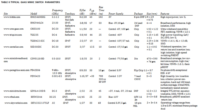
The typical parameters of some models with PIN-diode technology are shown in Table I.
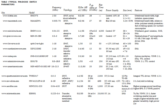
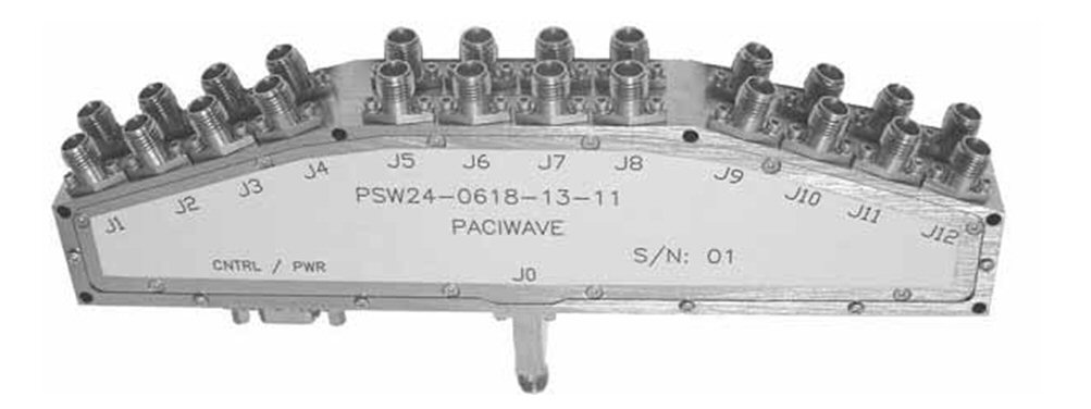
Figure 5. PIN SP24T switch model PSW24-0618-13-11 (Courtesy of Paciwave Inc.).
They differ by physical construction, architecture (e.g. from SPST to SP36T), operating frequency from 0.1 to 40 GHz, absorptive versus reflective configuration, power handling and switching time. Figure 5 shows an external view of a 6 to 18 GHz pin diode SP24T switch. It has 60 dB Isolation, 10 dB IL, 30 ns switching speed, and power handling of 100 mW average/2 W peak).
FET/GaAs Switches
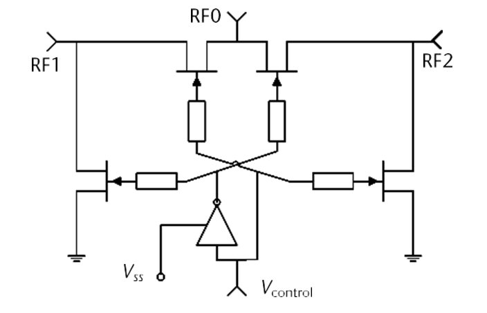
Figure 6. Typical block diagram of a FET switch.
A switching field-effect transistor (FET) is a three port device (see Figure 6), where the channel between source and drain ports forms a conduction path for the RF signal and the gate port controls whether it is blocked or passed. A DC control voltage applied between the gate and channel provides this function. FET switches offer relatively narrower bandwidths, lower power levels (less than 1W), lower loss (less than 0.8 dB), and higher isolation than PIN diode switches.
Manufacturers of solid-state switches use patented solutions for the drivers (logic circuits for the level of control signals to convert from a TTL or CMOS input voltage to the complementary drive signals required for GaAs FET switches with the appropriate operating speed). There are three basic elements in a GaAs FET driver circuit: the TTL input buffer section, a voltage translator, and complementary output buffer stages (see Figure 7). Separate driver’s ICs enable the matching of performance to requirements, such as linearization of the control characteristics. Drivers embedded into an IC provide minimal dimensions and minimal current consumption.
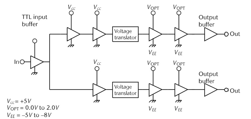
Figure 7. GaAs FET switch driver block diagram (Courtesy of M/A- COM Microelectronic Division).
Some parameters of MMIC solid-state switches in GaAs technology are shown in Table II. Solid-state switches using GaN technology are a promising development for high sitching speed switching, high switching power, good OFF-state isolation and low losses in the ON state.