
This article examines the factors driving the physical, electrical and cost constraints for 5G filters. To address these challenges, a narrowband filter design methodology using classic filter network theory, parameterized electromagnetic (EM) simulation and port-tuning techniques is presented. The approach is demonstrated using the NI AWR Design Environment platform to develop a narrowband 28 GHz bandpass cavity filter targeting mmWave backhaul applications.
5G will increase network capacity, reduce latency, and lower energy consumption through a number of innovative technologies aimed at enhancing spatial and spectral efficiency. The use of carrier aggregation, mmWave spectrum, base station densification, massive MIMO and beamforming antenna arrays will combine to support the goals of 5G communications at the cost of more signals operating in close spectral and spatial proximity. These enabling technologies place new demands on the filters required to mitigate signal interference across a dense network of base stations and mobile devices.
5G APPLICATIONS
5G will be deployed in stages to address three main thrusts; enhanced mobile broadband (EMBB), massive machine-type communication (mMTC) and ultra-reliable and low-latency communication (URLLC) for remote sensing and control for medical and autonomous vehicle applications. On the infrastructure side, densely-populated urban environments will utilize the mmWave frequency spectrum for higher data rates. Wireless backhaul is likely the most cost-effective and versatile solution to connect 5G base stations to the core network. Filters developed for the wireless backhaul application will face cost and volume challenges that must be considered early in the design stage.
DESIGN APPROACH AND FILTER SPECIFICATIONS
Ideal filter responses are well defined by math functions. This has led to the development of numerous commercial synthesis tools that can generate circuits for an exact filter response based on ideal element values; however, the parasitic behavior of the filter components must be considered early in the design stage. For this reason, synthesis is excellent for accelerating the initial design phase and generating mathematical filter solutions to serve as a starting point to define ideal lumped or distributed networks. Synthesis, however, is also limited in its ability to generate a physically-realizable filter. In this case, the synthesis tool provides critical coupling coefficients and external Q targets, but the ideal electrical design has limited usefulness.
Synthesis tools such as iFilter™ filter synthesis within NI AWR software can perform the math to produce ideal LC filters and precise distributed designs such as edge coupled, hairpin, interdigital and combline, based on ideal distributed microstrip and stripline models. Figure 1 shows several types of narrowband filters that can be synthesized based on microstrip technology with ideal distributed models that do not incorporate manufacturing limits and tolerances. Addressing these uncertainties can be very difficult without a process for converting ideal designs into physically-realizable ones.
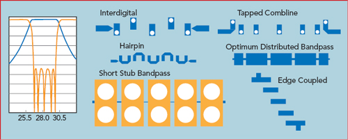
Figure 1 Several types of narrowband filters that can be synthesized based on microstrip technology.
The method used in this design is based on a technique introduced by Dishal and adopted for use with modern circuit and EM simulation by co-author Dan Swanson. EM modeling is used to efficiently determine three fundamental filter properties: the unloaded Q of the internal resonators, the coupling between two adjacent resonators and the external Q of the two resonators that form the input and output connections. Parametric studies with EM analysis are critical in modifying the physical structure in order to obtain specific values for these filter properties, which are determined by the Dishal method. Port tuning is then applied using circuit simulation and optimization with ideal lumped-element components, specifically, capacitors that are placed in strategic locations. Port tuning is used to guide adjustments that must be made to the final physical design.
Design by Optimization™
General purpose optimizers are not particularly efficient for filter design unless they are able to take advantage of the mathematical foundation that defines a filter’s optimal response. For a lossless Chebyshev filter, the optimal behavior is an equal ripple insertion and return loss response in the pass band. Thus, if the optimizer can consistently find this equal ripple response, optimization can reliably be used. The optimizer that is used in this project is available as an add-on module to the NI AWR Design Environment platform using the software’s API COM interface to integrate fully with Microwave Office circuit design software and AXIEM and Analyst™ EM simulators.
Designing a Physically-Realizable 5G Filter
The design methodology follows a set of well-defined steps that scale for the desired frequency and bandwidth (see Figure 2). The process starts with specification of the filter requirements, including bandwidth, passband return loss and stopband rejection, from which the filter order is determined and the lowpass Chebyshev parameters are determined and scaled to the required frequency.

Figure 2 Steps for designing a physically-realizable 5G filter.
An EM model of a single resonator is built, and its length for a desired resonant frequency and unloaded Q is determined. Additional EM models are created to generate the coupling coefficient and external Q curves that guide the determination of key physical dimensions such as resonator spacing and tap height. These individual components are then assembled, and port tuning is used to tweak the design for the optimum equal ripple response using optimization.
Narrowband Bandpass Filter Design
The filter is designed with a center frequency of 28 GHz, (3GPP band n257). The construction is based on a single in-line cavity using an interdigital arrangement to achieve 30 dB of rejection at 800 MHz off center frequency and an in-band return loss of 20 dB. This sets the in-band ripple at 0.044 dB. From these specifications, the expected insertion loss and the necessary filter order are determined.
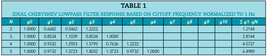
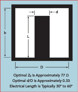
Figure 3 Coaxial resonator cross section.
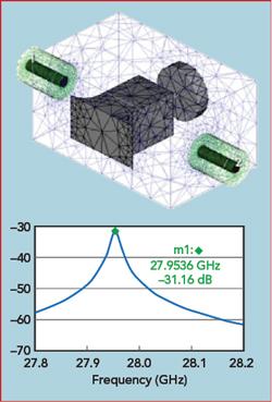
Figure 4 Coaxial resonator EM model.
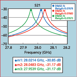
Figure 5 EM resonator simulation results for different resonator lengths.
The mathematical foundation for an ideal filter response is well established, with parameter values derived for an ideal lowpass Chebyshev filter response based on a cutoff frequency normalized to 1 Hz (see Table 1). Once the prototype ripple level is determined from the desired in-band return loss, the filter order N can be estimated based on the desired stopband rejection, as shown in Equation 1. A fifth-order filter is needed to achieve the desired selectivity and bandwidth.
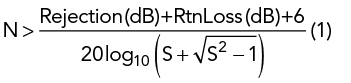
Where:
Rejection = Stopband Insertion Loss
RtnLoss = Passband Return Loss
S = Rejection Bandwidth/Filter Bandwidth
Design Details
The design is based on an interdigital configuration made up of coupled resonators with the open ends on a substrate or cavity alternately pointing in opposite directions. The length of the resonators determines the resonant frequency and the coupling between resonators is controlled by their separation. The width of the housing, for a cavity filter should be λ/4 at the operating frequency.
In addition to the cavity dimensions, another early concern is determining the cross-sectional dimensions of the resonator post. The resonator post cross section in relation to the outer cavity wall determines the characteristic impedance of the resonator. For a coaxial resonator, literature indicates an optimum resonator characteristic impedance of around 77 ohms, as determined by the resonator cross-section, resulting in a post-to-cavity width ratio of about 33 percent (see Figure 3). In this case, the optimum unloaded Q (Qu) is not achieved due to physical constraints. A coaxial transmission line calculation approximates the resonator Zo ~46 ohms.
Resonant Frequency and Qu Simulation
With the cavity and resonator cross-section dimensions determined, an EM model of a single resonator is defined with the resonator length parameterized so that the resonant frequency can be controlled, as shown in Figure 4. The EM model uses two coaxial feed structures that are loosely coupled to the waveguide cavity to act as the input and output ports. The frequency response for several different resonator lengths (see Figure 5), demonstrates that the resonant frequency increases with a shortening of the resonator.
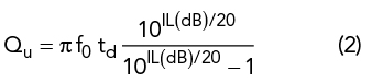
The Qu of an individual resonator is calculated from the simulated time delay and insertion loss using Equation 2.
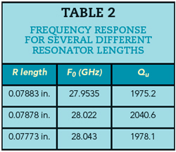
For lowpass Chebyshev parameters, center frequency, and simulated Qu are shown in Table 2. An expected insertion loss of approximately 0.25 dB is calculated for the entire filter at mid-band using Equation 3.
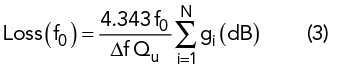
Where:
Δf is the equal ripple bandwidth of the filter
Qu is the expected average unloaded Q for the resonators
gi are the normalized lowpass filter element values, calculated for a given ripple in the Table 1.