
Symmetry is an element of beauty. Besides it's esthetic appeal, symmetry is practical. Symmetry has two important manifestations in electric-wave filters: symmetry with respect to element values mirrored about the input and output (physical symmetry) and symmetry in the responses mirrored about the center frequency of bandpass filters (response symmetry).
For lumped-element filters, physical symmetry results in the reduction by a factor of two of the number of unique elements that must be designed, modeled, purchased, tested, stocked and picked for assembly. This leads to savings in both design and manufacturing effort. For distributed-element filters that are simulated using electromagnetic simulation, physical symmetry can reduce the required execution time and memory by as much as a factor of sixteen if the simulator takes advantage of symmetry. Electromagnetic simulation of complex circuits might not be feasible without this memory reduction, while the increased execution speed often reduces simulation time from hours to minutes.
Response symmetry is particularly desirable for IF filters. Conventional exact transform bandpass filters have a symmetrical response when plotted on a logarithmic frequency scale (geometric symmetry); however, it is typically arithmetic symmetry (a plot on a linear frequency scale) that is desirable. Arithmetic symmetry also results in symmetry in the group-delay. Symmetry in the group-delay response results in simplified group-delay equalizer design.
PHYSICAL SYMMETRY
Physical symmetry results naturally, without additional user effort, in filter types that are: (1) Butterworth, (2) odd-order Chebyshev and (3) coupled-resonator bandpass filters. It also is present in (4) low pass filters with finite transmission zero pairings and an odd quantity of zeros at infinity, and (5) bandpass filters with finite transmission zero pairings above or below (not both) the passband and with odd and equal quantities of zeros at DC and infinity (for example, 3 zeros at DC, 3 at infinity and 2 at equal frequency below the passband).
Physical symmetry maybe forced by (6) optimizing the response while forcing symmetry.
The design of types 1 through 3 is straightforward using well-known routines.1 These are restricted to all-pole filters. Types 4 and 5 with finite transmission zeros require direct synthesis techniques. Type 5 is useful when an asymmetric response is required, such as high selectivity on one or the other side of the passband. The design of type 6 benefits from the integrated synthesis and simulation environment provided by GENESYS 7.5.2 The design of physically symmetric filters will be illustrated for the type 4 low pass.
|
|
A LOW PASS WITH FINITE ZEROS AND PHYSICAL SYMMETRY
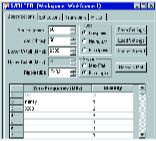
Consider the =S/FILTER= specification tab of a 2300 MHz low pass filter shown in Figure 1. All-pole low pass filters have all zeros of transmission at infinite frequency. To improve selectivity this filter includes transmission zeros at finite frequency. The placement of zeros conforms to the rules of type 4: the number of zeros at infinity is odd (1) and finite zeros are paired at 3800 MHz.
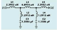
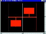
The schematic for the low pass is shown in Figure 2. Note the symmetry of the component values mirrored about the center 4.8914 nH inductor.
CONVERTING THE 2300 MHz LOW PASS TO DISTRIBUTED
This example illustrates how to realize the previous 2300 MHz low pass with distributed elements. The inductors are replaced with high impedance transmission lines3 using the formula
Z0 = ωL/sin
where
Z0 = characteristic impedance of the line
= electrical length of the line
ω= cutoff frequency in radians of the low pass filter
A higher impedance line results in shorter lengths thus improving the equivalence of a line to a lumped inductor.
The capacitors are replaced with low impedance lines3 using the formula
Z0 = sin /ωC
The series inductors are replaced with 10 mil wide lines and the shunt capacitors are replaced with 280 mil wide lines. The substrate parameters are
Er = 2.55
Tan = 0.0004
Rho = 1
Roughness = 0.055
Tmet = 0.71 mils
H = 31 mils
Using =T/LINE= the 10 mil wide lines are found to have a characteristic impedance of approximately 135 Ω and a full wavelength is 3733 mils at 2300 MHz. The 280 mil wide lines have a characteristic impedance of 20.7 Ω and a full wavelength is 3380 mils. The equivalent distributed structure is then shown in Figure 3 with the following dimensions
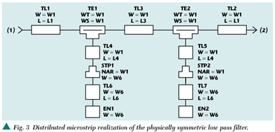
L1 = ?156
L3 = ?329
L4 = ?82.9
L6 = ?211
W1 = 10
W6 = 280
|
|
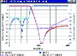
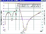
The effects of discontinuities are included by adding tee, step and end models. The lumped to distributed equivalents are only approximate and the discontinuities impact the response as well. All line lengths were therefore optimized using the circuit theory simulator =SUPERSTAR= to obtain the best response. The transmission and reflection plots with circular and square markers, shown in Figure 4, are for the original symmetric low pass filter. The triangular and diamond markers are plots of the distributed low pass after optimization. The degraded stopband performance of the distributed filter above 5000 MHz is a natural limitation of distributed filters and is due to re-entrant modes.
Next =LAYOUT= is used to create a layout of the filter. This same layout is used to export a Gerber file for manufacture and as a complete circuit description for the electromagnetic simulator =EMPOWER=. The layout is given in Figure 5. Note the second series L-C to ground was turned upward, resulting in 180° rotational symmetry that is even more efficient than mirror symmetry about the center. =EMPOWER= automatically performs an electromagnetic analysis of this layout.
The responses of the circuit theory simulation in =SUPERSTAR= and the =EMPOWER= simulation are shown in Figure 6. This exceptional correlation is not always achieved because =EMPOWER= often reveals limitations associated with circuit theory simulation.
RESPONSE SYMMETRY
None of the popular low pass to bandpass transforms have arithmetic symmetry. The conventional bandpass filter with alternating series and shunt resonators has an equal number of transmission zeros at DC and infinite frequency. For example, a 3-section (6th-degree) bandpass has 3 transmission zeros at DC and 3 at infinity. Carassa4 proved that if the number of transmission zeros at infinity is 3 times the number at DC then the response can be symmetric. This can be maintained even with the addition of transmission zeros at finite frequencies. The conventional bandpass has too few zeros at infinity in relation to the number at DC and therefore too little selectivity above the passband to be symmetric.
Blinchikoff5 described a flat group-delay bandpass that satisfied Carassa's criteria but it is only available for third-order all-pole filters of 30 percent to 70 percent bandwidth. In 1989 a low pass to bandpass transform was developed that complied with Carassa's rule and resulted in arithmetic symmetry. Rhea3 described this transform in more detail. However, this transform is approximate and is available only for all-pole filters.
The direct synthesis routines in =S/FILTER= offer a more elegant solution to this problem because the user may specify all infinite and finite transmission zero frequencies. The following example illustrates how to design bandpass filters with arithmetic response symmetry.
A FILTER WITH RESPONSE SYMMETRY
|
|
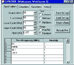
The specifications tab for a 70 MHz IF filter with 30 MHz bandwidth is shown in Figure 7. Notice that the quantity of zeros at infinity is 3 times the quantity at DC. Finite transmission zeros were added above and below the passband to improve selectivity. They were manually tuned to 38.7 and 103.2 to achieve a minimum attenuation in the stopband of 42 dB.
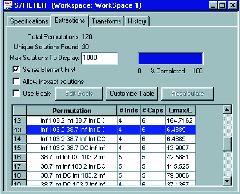
The four non-finite and two finite zeros may be extracted in a number of different sequences. The =S/FILTER= Extraction tab shown in Figure 8 illustrates there are 120 possible permutations of extraction sequence, and 30 unique and different possible filter topology schematics.
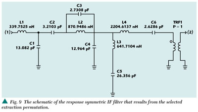
The extraction sequence  103.2 38.7 DC was selected because it contained the fewest number of inductors (4) and had a desirable maximum to minimum ratio of inductor values (6.48888) thus improving realizability. The resulting schematic is shown in Figure 9.
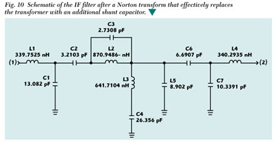
=S/FILTER= includes built-in transforms to manipulate a topology to one that is more desirable. Here it is desired to remove the transformer and the following transforms were applied.
1) C4 was swapped with L3/C5
2) L4 was swapped with C6
3) A Norton Series was applied to C6 using the option "Calculate N to remove existing transformer"
4) Simplify Circuit was clicked
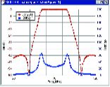
The final schematic is shown in Figure 10. Notice the transformer is removed and the inductor ratio is reduced to 2.56 (L2/L1). If this filter were realized using a conventional elliptic filter the response would not be symmetric, 5 inductors rather than 4 would have been required and the minimum to maximum inductor ratio would exceed 8. The response for this remarkable filter is shown in Figure 11. Notice the excellent transmission and amplitude and group-delay symmetry.
PRACTICAL ISSUES
|
|
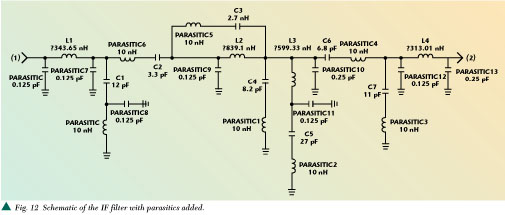
The previous filter has non-standard component values and ignores parasitic effects. Converting a theoretical design to a more realistic design that considers standard values and parasitics is illustrated next. This is best classified as an activity because it involves procedures that rely not only on theoretical concepts but also the user's knowledge of the components. One of this author's work responsibilities is to influence the development of products to optimize their usefulness from the engineer's perspective. However, regardless of the sophistication of a software suite, a skilled designer will leave his creative mark on circuits. Parasitics are strongly influenced by the choice of components and their environment. The set of steps described here should be interpreted broadly.
Only one set of component values resulting from each specific extraction sequence realizes the exact transfer function. A Norton transform may be applied to the filter to change the internal impedance level of the filter to make a specific component a standard value. This may be applied repeatedly from left to right until each component is a standard value. However, each Norton transform application adds a component to the design, therefore doubling the number of elements in the filter. Furthermore, the termination impedances are modified.
One may select nearby standard values and accept a degraded response. However, the presence of parasitics makes standard values an idealistic concept. Furthermore, acceptance of a compromised response is subjective. One designer might choose the next highest standard value while another might choose the next lowest standard value based on response objectives.
There is more freedom in dealing with these issues than might at first be imagined. Only three basic principles define a bandpass filter. First, resonators must exist. Secondly, the resonators must be coupled and third, the end resonators must be coupled to the terminations. The response is naturally more sensitive to the individual resonator frequencies than to coupling values. Therefore, since the frequency a resonator operates at may be adjusted by either the capacitor or the inductor, a strategy of setting the frequency by adjusting either the capacitor or inductor is generally successful. In other words, setting all capacitors on standard values and using tunable inductors, or vice versa, works well.
Both standard values and parasitics disturb the ideal response. An effective procedure is to deal with both issues simultaneously using optimization. Our strategy here is to add parasitics to the simulation, set capacitors on standard values and optimize the inductors to recover the response.
The filter will be constructed with leaded capacitors and inductors. The estimated inductance in series with each capacitor is 10 nH and the capacitance associated with the inductor is modeled as 0.125 pF to ground at each end of the inductor. Figure 12 shows the final schematic with parasitics added, standard capacitors and optimized inductor values. The inductors are not standard values because the strategy was to use tunable inductors.
|
|
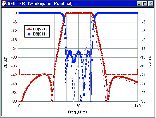
Figure 13 shows the responses before (dashed) and after (solid) optimization. The primary effect of standard values and parasitics was degradation of the return loss. The degradation here is moderate. Higher frequencies, better return loss and narrower bandwidth increase component sensitivity and realistic designs often result in more severe degradation. In this case, optimization improved the return loss from 11 to 13 dB. *
References
1. G. Matthaei, L. Young and E.M.T. Jones, Microwave Filters, Impedance-matching Networks and Coupling Structures, Artech House, Norwood, MA, 1980.
2. GENESYS Version 7.5 Operation Manuals, Eagleware Corp., Norcross, GA, 2000.
3. R. Rhea, HF Filter Design and Computer Simulation, Noble Publishing, Atlanta, GA, 1994.
4. F. Carassa, "Bandpass Filters Having Quasi-symmetrical Attenuation and Group-delay Characteristics," Alta Frequenza, July 1961, p. 488.
5. H. Blinchikoff and A. Zverev, Filtering in the Time and Frequency Domains, Krieger Publishing, Malabar, FL, 1987.
 Randall Rhea has degrees from the University of Illinois and Arizona State University. He worked at the Boeing Company, Goodyear Aerospace and Scientific Atlanta, where he was appointed Principle Engineer in 1985. In 1985, Randy founded Eagleware Corp., developer of the analog, RF and microwave design tool GENESYS, with thousands of users worldwide. In 1994, he founded Noble Publishing. Randy is the author of numerous technical articles and the books Oscillator Design and Computer Simulation and HF Filter Design and Computer Simulation. He is also the author of Chapter 6 of the Handbook of Microwave Technology. He is the author of the original versions of four programs in the GENESYS software suite. For a decade he has taught workshops worldwide at trade shows and within corporations.