
A Linear LDMOS Amplifier for 3GPP Applications
Philips Semiconductor
Foxboro, MA
With the introduction of digital modulation formats and the trend towards multi-carrier amplifiers, base station power amplifiers require the use of transistors with high peak power capability. The amplifier is required to meet stringent linearity requirements. For that reason second generation LDMOS die technology was introduced in early 2000. When designing LDMOS die, it is important to create a good compromise between peak power capability and Idq drift characteristics, while maintaining good performance on other important RF characteristics such as gain, efficiency and thermal resistance of the transistor. This article introduces the model BLF2022-90 linear base station amplifier for the 2110 to 2170 MHz frequency band. The BLF2022-90 is a single-ended 90W N-channel enhancement-mode laterally diffused MOS-FET transistor which is suitable for use in multi-carrier wideband-CDMA (W-CDMA), Universal Mobile Telecommunications System (UMTS) and Third-generation Partnership Project (3GPP) applications. Integrated input and output matching make it easy to create an amplifier design with excellent gain flatness (gain equals approximately 14 dB; gain flatness < 0.1 dB from 2110 to 2170 MHz) and phase linearity (< 1° from 2110 to 2170 MHz), two critical parameters when designing feed-forward amplifiers. The BLF2022-90 is available in both a standard as well as an earless SOT502 package; the latter allows for the device to be soldered to a heatsink, which will greatly improve the thermal resistance between device and heatsink.
|
|
RELIABILITY
Reliability of RF power amplifiers is a key issue. Reliability and/or device lifetime is affected to a large extent by the device junction temperature. The thickness of a transistor die, die layout, transistor package and device efficiency are the main parameters that effect the device junction temperature. Furthermore, it is well-known that gold top metallization in combination with gold bond wires greatly enhances device reliability, a combination which is used in all Philips Semiconductors' LDMOS transistors. Use of something other than gold top metallization will reduce the device lifetime, when no other precautions in the die design are taken. The BLF2022-90 has a thermal resistance from junction-to-(transistor) case (Rth,j-c ) of 0.59 K/W. For example, when the device is operated with a 3GPP signal at an average output power of 10 W the efficiency is approximately 15 percent. Thus, the required DC input power is 67 W. The dissipated power at that operating point is approximately 57 W. Therefore, the increase in temperature between the case and transistor junction is 57 W * 0.59 K/W = 33.7°C. This means that when the transistor case temperature is 85°C the actual device junction temperature is 118.7°C, which is well below 150°C, a design rule which is maintained as normal in this industry.
With electromigration being the dominant failure mechanism for the BLF2022-90, the device still has an expected lifetime of well over 1E07 hours, according to Black's formula for devices with a gold top metallization. An increase in device junction temperature exponentially reduces the device lifetime, according to Black.
DEVICE CONSISTENCY
Another key aspect, underestimated by many, is device consistency. Device consistency starts with the consistency of the active element, the die. The second element is the device assembly, that is, consistent placement of the die, integrated MOS capacitors, and shape and length of the gold bond wires which connect these tiny components inside the transistor package to each other and to the leads of the transistor package. All of these parameters are controlled by automated machines in diffusion and assembly locations. In the end the user benefits from those well controlled processes, which for them means minimal tuning in the application circuits when they use device after device.
RF PERFORMANCE CHARACTERISTICS
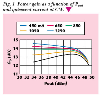
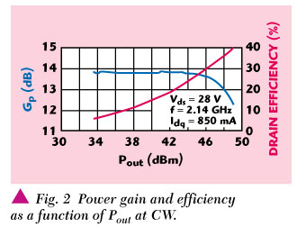
Typical performance of the BLF2022-90 device in a 3GPP application circuit operating at 28 V and Idq = 850 mA over the 2100 to 2170 MHz frequency range is as follows: A 3GPP test signal with 15 DPCH and a peak-to-average ratio of 9.5 dB at 0.01 percent probability and a channel bandwidth of 3.84 MHz was used to drive the device. The LDMOS amplifier displayed an output power of 40 dBm and an efficiency of 15 percent. The device showed a gain of 13.85 dB at 2140 MHz with a gain flatness of 0.02 dB over the 2110 to 2170 MHz bandwidth. Figure 1 shows the device's power gain as a function of power output and quiescent current under CW conditions. Figure 2 shows power gain and efficiency vs. power output. Nominal delay was 2.07 ns and phase linearity was 0.45° over the 2110 to 2170 MHz band. Input return loss was greater than 14 dB over the same bandwidth.
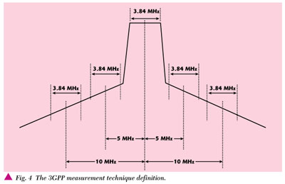
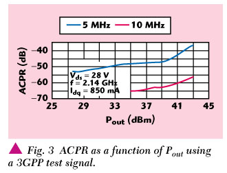
The device has an ACPR of 45 and 62 dBc at 5 and 10 MHz, respectively, using an integration bandwidth (IBW) of 3.84 MHz. Figure 3 shows the ACPR as a function of power output, and Figure 4 shows the 3GPP measurement technique definition used for the ACPR analysis. A complete application note is available by contacting Paul Wilson at Paul.Wilson@philips.com or Korne Vennema at Korne.Vennema@philips.com.
Philips Semiconductors,
Foxboro, MA 508-851-2230.
Circle No. 300