
Control Products for Wireless and Broadband Applications
Alpha Industries Inc.
Woburn, MA
 Switches, attenuators, directional detectors, phase shifters and other GaAs and silicon devices are shrinking dramatically as suppliers are challenged to develop new process and packaging techniques. Customers are demanding that new devices operate with a higher degree of linearity and maintain performance at low battery voltages, while still driving integration up and costs down.
Alpha Industries is responding to these market demands. As a leading manufacturer of GaAs ICs and silicon discretes used in current wireless, broadband and third-generation (3G) designs, the company is integrating multiple functions into components that cost less and take up less space on a PCB. For example, the new 25 mm2 model AA107-310 digital attenuator replaces two separate components previously requiring over 100 mm2 of board space. This represents a four-to-one reduction in real estate.
This article describes some of the innovations resulting from combining the company's core competencies in circuit design, silicon and GaAs semiconductor manufacturing, process integration and packaging. It also touches on products under development to demonstrate the company's ability to provide the technology needed to support the next generation of wireless and broadband applications.
BASE STATION INNOVATIONS
RF GaAs IC Switches
Significant package size reduction has been achieved on many RF GaAs IC switches. The model AS196-307 high isolation GaAs SPDT switch with integrated silicon ASIC 1:2 decoder (shown in the photo above) is packaged in a 4 * 4 mm leadless plastic chip carrier (LPCC-16) exposed-pad package. Very high isolation is achieved by soldering the exposed paddle directly to the PCB ground. Lead inductance is reduced from 2 nH (1 nH/lead) to approximately 0.4 nH (0.2 nH/lead).
The AS196-307 requires only a positive supply voltage (VCC = 3 to 5 V) and one CMOS-compatible control line (VCTL = 0 to 3/5 V). A logic 0 is equal to 0 to 0.5 V while a logic 1 is equal to 3.5 to 5 V with VCC = 5 V. Insertion loss is approximately 1 dB, I/O SWR < 1.4 and isolation 55 dB up to 2 GHz, 40 dB at 4 GHz and 30 dB at 6 GHz, as shown in Figure 1. These characteristics make the AS196-307 switch ideal for applications requiring high isolation such as in 2G, 3G, base station LO switching, U-NII time division duplex transceivers and WLL radios.

Digital Attenuators
New packaging is also reducing the size of voltage variable digital attenuators. For example, a silicon ASIC serial-to-parallel converter has been integrated with a GaAs attenuator IC in a single micro lead frame 5 * 5 * 1 mm exposed-pad package (MLF-32). Figure 2 shows the attenuator's pinout diagram. The model AA107-310 attenuator takes up just 25 mm2 on a PCB. Older designs required two separate packages taking up over 100 mm2 .

The AA107-310 attenuator is a 5-bit device with 0.5 dB steps to 15.5 dB total attenuation with low insertion loss and high bit accuracy, as shown in Figure 3. It is designed for use as a gain control element in the IF sections (< 500 MHz) of base station radios and is to be used with a reverse path amplifier in broadband systems. Insertion loss is 1 dB, bit accuracy is < ±0.3 dB and SWR is < 1.4 below 500 MHz.

The silicon ASIC performs serial-to-parallel data conversion eliminating the need for individual bit control. Only three inputs are required: serial clock and data, and latch enable. The reset pin can be tied high for truth table control or low for master reset to the insertion loss state. A single positive supply voltage (VCC = 5 V) and three external capacitors are required, one for VCC bypassing, one for a charge pump (C1 , C2 ) and one for negative voltage holding. An on-chip negative voltage generator (f = 600 kHz) allows direct control of a standard GaAs attenuator IC eliminating the need to float ground connections.
The model AA109-310 is another new digital attenuator that integrates a silicon ASIC serial-to-parallel converter with a GaAs attenuator IC. It is a 5-bit device with 1 dB steps to 31 dB total with low insertion loss and high bit accuracy. It is designed for use as a gain control element in the RF sections (> 500 MHz) of base station radios. Insertion loss is 2 dB, bit accuracy is < ±0.5 dB and SWR is < 1.8.
The silicon ASIC performs the same function for this device without the negative voltage generator. The GaAs IC is floated on-chip eliminating the need for a negative voltage. The package is the same as the AA107-310 device.
High Dynamic Range Voltage Variable Attenuators
A family of GaAs FET-based low cost, low current, high dynamic range voltage variable attenuators (VVA) has also been developed. Applications are as gain control elements in low power, wireless and broadband systems. They are controlled with a single positive voltage (3 to 5 V) with linear attenuation vs. voltage. Dynamic range is greater than 35 dB. Models AV105-12, AV109-73 and AV110-73 are typical of these devices.
Low Distortion Voltage Variable Attenuators
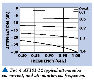
The distortion performance of the traditional GaAs FET-based VVA is a primary limitation in large signal handling at base stations. The company's solution is based on its GaAs passive IC quadrature hybrid structure technology, low distortion silicon PIN diode design and the small footprint SOIC-8 package. The new HIP3™ attenuator product line comprised of models AV101-12 and AV111-12 (0.8 to 1.0 GHz), AV102-12 and AV112-12 (1.7 to 2.0 GHz), and AV113-12 (2.1 to 2.3 GHz) covers the wireless bands.
For example, the AV111-12 VVA operates at between 0.8 to 1.0 GHz, integrates two silicon PIN diodes and a quadrature hybrid, and operates with an IP3 guaranteed better than 37 dBm. This performance is approximately a 20 dB improvement over a GaAs MMIC-based VVA. Other performance specifications are equally impressive, with an attenuation range higher than 20 dB and a 1.5 dB insertion loss. The AV111-12 is actually a current-controlled attenuator, but it achieves its specified dynamic range with no more than 1.2 mA. Table 1 lists the AV111-12 VVA's electrical specifications. Figure 4 shows the AV102-12 VVA's typical attenuation vs. frequency characteristics.

HANDSET INNOVATIONS
RF GaAs IC Switches
Device integration and packaging are critical in handset switches. The AS190-73, AS191-73 and AS193-73 family of PHEMT SPDT switches provide extremely high linearity at low control voltages for handset applications. Table 2 lists the performance trade-offs for each part. These parts all have the same package, pinout and truth table.

The model AS198-306 is a new high power PHEMT SP4T switch with integrated silicon 3:5 decoder in a MLF-16 4 * 4 mm exposed-pad package. The switch has excellent linearity performance at low voltages. Typical second- and third-order harmonics are 65 dBc at 900 MHz and 3 V. Designed for dual-band handset applications, the AS198-306 has low TX path insertion loss (0.6 dB at 900 MHz) and good RX isolation (25 dB at 900 MHz), as shown in Figures 5 and 6, respectively. The integrated silicon decoder reduces the number of positive control lines to three. If used in the 2:4 configurations two control lines can be used.


Directional Detectors
Another innovation combines passive circuit design and semiconductor technology in a monolithic structure that integrates a GaAs directional coupler with GaAs Schottky diodes for use as a broadband detector used as an automatic gain control element. The model DD01-92 directional detector is packaged in a single miniature SC-88 (six lead SC-70) plastic package and operates from 650 MHz to 2.4 GHz. The DD01-92 may be conveniently temperature compensated due to the closely matched pair of Schottky diodes. The monolithic construction of the detector consists of two Schottky diodes and a terminated directional coupler. This product features both small size and low cost, making it appropriate for high volume handset applications.
Figure 7 shows the detector's circuit configuration, and Figures 8 and 9 show the device's differential detected voltage, and insertion and return losses vs. frequency, respectively.


IN DEVELOPMENT
A variety of new control products are currently in development to meet market demands for smaller, more reliable devices. These new products include RF diodes in chip-scale packaging, vector modulators, amplitude phase shifters and low distortion digital attenuators.
Chip-scale Packaging of RF Diodes and GaAs RF ICs
To meet the market demand for smaller components, the company is developing the technologies to produce virtually package-less devices that will be compatible with current pick-and-place insertion techniques. Using cost-efficient, batch-scale processing, which eliminates the need for wire bonding, chip-scale technology creates surface-mountable diodes with dimensions of less than 30 mils (0.7 mm) per side and smaller than 15 mils (< 0.4 mm) in height. This marks a significant height reduction compared to the widely-used 0.7 mm height of the SC-79 package.
Because of its low parasitics, chip-scale PIN diodes in switch and attenuator circuits show a significant improvement in frequency performance in comparison with plastic-packaged parts. A primary limitation to the performance of a broadband control circuit working above 5 GHz has been the parasitic package inductance of the plastic-packaged PIN diodes. The inductance of the chip-scale PIN diode is expected to approach 0.1 nH compared to 0.7 nH for the SC-79 package shown in Figure 10.

The company's smallest present GaAs RF IC switch package is the 2.2 * 2.0 mm footprint of the SC-70. The chip-scale version reduces this area to 1.5 * 1.0 mm. This package is leadless with backside land grid contacts. The lower package inductance yields higher switch isolation and frequency response. Future chip-scale plans also include Schottky and varactor diodes, as well as integrating multiple semiconductors -- including amplifiers, switches and driver circuits -- on a discrete chip.
VECTOR MODULATOR
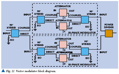
A series of vector modulators are in development to cover the wireless bands. These devices utilize existing monolithic quadrature hybrids, power dividers, FETs and PIN diode chips to create devices designed to adjust the phase and amplitude of an RF signal. This results in a very small (1 cm2 ) BGA module. Vector modulators are similar to I & Q modulators, but unlike some basic monolithic I & Q modulators, they provide a linear path for the RF signal. With a vector modulator, the RF signal is not amplitude-limited because the output RF power is always proportional to the input RF power. This feature is widely used in feedforward or feedback loops of multi-channel power amplifiers to cancel distortion. The new vector modulator design has approximately 15 dB loss and an accuracy of better than 4° over a control range of 10 dB. Figure 11 shows the vector modulator's block diagram.
Amplitude and Phase Shifter
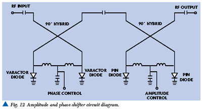
An amplitude and phase shifter (APS), shown in Figure 12, is also in development. This small (1 cm2 ) ball grid array module will accomplish the same task as a vector modulator, but is less complex and operates with less loss (9 dB). Amplitude variation is 1 dB over 360° of phase shift. The APS is controlled by separate phase and amplitude signals whereas the vector modulator is controlled by separate in-phase and quadrature control signals.
Low Distortion Digital Attenuator
Six-bit attenuators for both the wireless infrastructure and broadband markets are under development as well. They feature a least significant bit of 0.5 dB with a total attenuation of 31.5 dB. This broadband, high linearity device is designed to achieve greater than 60 dBc second harmonic performance at a 5 MHz fundamental frequency.
CONCLUSION
Due to manufacturers looking for a differentiating advantage in a growing, complex market, the current generation of wireless and broadband devices will probably be obsolete in a year or two. One mobile telephone company is even promising new subscribers a replacement phone every two years. Handset product features are blurring as multimedia devices take on the roll of handsets and handsets incorporate features of multimedia devices.
The next generation of handsets -- already under development -- may contain three or four radios operating in the cellular, PCS and 3G spectrum, while incorporating Bluetooth functionality. Building components for products like these leverages the company's strengths in advanced semiconductor and hybrid process technology, innovative circuit design and modeling, and state-of-the-art packaging.
Alpha's capabilities go beyond manufacturing highly reliable RF GaAs ICs, discrete semiconductor devices and passive components. Working with leading handset and base station equipment manufacturers, the company is creating the innovative solutions needed to implement a new generation of wireless devices and has demonstrated its ability to integrate multiple components and functions in ever-smaller packages. With its proven high volume, low cost production capabilities, innovative products to meet the growing demand for ultra-high speed, high capacity, data and voice wireless communications are being developed. For additional information, visit the company's Web site at www.alphaind.com.
Alpha Industries Inc.,
Woburn, MA
(781) 935-5150.