
The next generation mobile network, 5G, is envisioned as a flexible, efficient and resourceful platform offering advanced capabilities that will form the core of future use cases and new businesses opportunities. While these future applications are impossible to predict, they will depend on connectivity to a new radio access network that provides higher bandwidth, ultra-high reliability and low latency. Today, only a few 5G services have been identified; the most promising are fixed wireless access (FWA) and enhanced mobile broadband (eMBB) services.
To meet the multiuser demands of FWA and eMBB, network operators are planning to deploy microcell/picocell access points that use active antenna arrays and beamforming to precisely control high bandwidth connections. These active array solutions rely on multiple RF transmit/receive (Tx/Rx) chains to form and scan the beams, with the spacing between each antenna one-half the wavelength (λ/2). With increasing transmit frequency, the spacing between antennas becomes quite small; e.g., for a 28 GHz antenna array, the spacing is 5 mm. The limited area for component placement and the Tx/Rx performance requirements for mmWave antenna arrays creates an entirely new set of challenges for the semiconductor technology used in the front-ends.
HYBRID BEAMFORMING
The literature contains numerous studies evaluating digital, analog and hybrid beamforming architectures, offering multiple perspectives.1-3 Ultimately, the architecture choice depends on the power consumption, cost and performance requirements for the access point. Hybrid beamforming is emerging as the favored architecture for mmWave active antennas, as it enables using the optimum semiconductor technologies across the system. A simplified block diagram of such a system2 is shown in Figure 1, which also shows the preferred semiconductor technologies for the functional blocks.
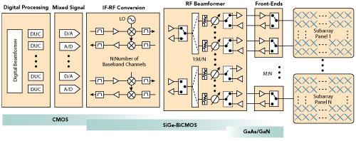
Figure 1 Simplified block diagram of mmWave phased array using hybrid beamforming.
An important trade-off is between array size (the number of antennas) and total array power consumption. This trade-off is driven by the transmit power of each antenna element, determined by the semiconductor technology employed for the front-end power amplifier (PA). An excellent illustration of this is shown in Figure 2, which represents a 28 GHz system with 60 dBm effective isotropic radiated power (EIRP).1 The takeaways from these graphs are:
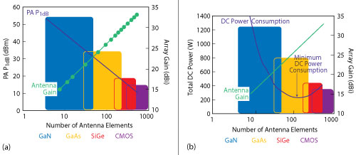
Figure 2 Phased array trade-offs: PA output power (a) and array DC power consumption (b) vs. number of antenna elements to achieve 60 dBm EIRP, with overlay of semiconductor technology capabilities.
- The target EIRP can be satisfied with a wide range of PA power levels, as shown in Figure 2a,
- Antenna gain increases with the number of elements, also shown in Figure 2a and
- As the number of antenna elements increases, with lower transmit power per element, the total array DC power decreases, reaching a minimum at approximately 128 elements, then increases, as shown in Figure 2b.
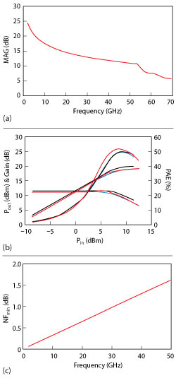
Figure 3 PIH1-10 GaAs process performance: MAG of 2 x 50 µm PHEMT unit cell with VD = 4 V and VG at 100 mA/mm ID (a); 2 x 75 µm unit cell gain, output power and PAE vs. input power at 29 GHz, with VD = 4, 5 and 6 V (b); 4 x 25 µm PHEMT noise figure vs. frequency with VD = 2 V and VG at 100 mA/mm ID (c).
As more antenna elements are added to accommodate the lower P1dB available from SiGe and CMOS PAs, more power is consumed by the front-ends and beamformer ICs that feed and control these channels. One example of this is a fully integrated, dual polarized, 28 GHz, SiGe beamformer IC with 16 elements.4 With a die size over 160 mm2, the majority of which is the front-end, this component consumes a considerable amount of silicon. One may extrapolate this to an array of several hundred antenna elements and quickly realize the cost, size and assembly challenges that result from a suboptimal choice of front-end semiconductor technology.
This analysis of the effect of front-end semiconductor technology on the total power consumption of the array shows that a GaAs PA will result in the minimum power consumption. The cited literature contains additional studies of active array antenna systems and reaches similar conclusions that GaAs represents the optimum technology choice for mmWave front-ends. These references acknowledge GaAs can provide the optimum range of PA performance but claim GaAs cannot fit within the λ/2 antenna spacing of the antenna elements (e.g., 5 mm at 28 GHz). Historically, multifunction integration has been a weakness for GaAs technology, particularly for short gate length processes used at mmWave.
INTEGRATED GaAs
Owing to its dominant share of cellular and Wi-Fi RF front-ends used in mobile devices, GaAs manufacturing continues to advance and now offers best-in-class performance and the integration required for mmWave active antenna systems.
Long ago, the mmWave performance of GaAs PHEMT devices exceeded the optimum power levels needed for FWA active antenna arrays; however, a more advanced platform was required to satisfy the spacing requirements. To meet the size requirements of mmWave active antenna arrays and provide additional capabilities for more complex applications, advanced compound semiconductor manufacturers now offer innovative GaAs PHEMT technologies that monolithically integrate the Tx PA, Rx LNA and low loss PIN switch in a single chip mmWave front-end. In addition to these functions, platforms like WIN Semiconductors’ PIH1-10 provide a linear Schottky diode for power detectors and mixers, low capacitance PIN diodes for ESD protection and optimized E/D transistors for logic interfaces. This suite of capabilities comes in a humidity-rugged back-end, available with a copper redistribution layer and copper pillar bumps to reduce die size and allow flip chip assembly, enabling GaAs front-ends to fit within 28 and 39 GHz antenna lattice spacing.
mmWAVE PERFORMANCE
The core of these integrated technologies is a versatile enhancement-mode PHEMT transistor that provides excellent power, gain, power-added efficiency (PAE) and noise figure at mmWave frequencies and is biased from a single positive supply. Figures 3a and b show measurements of the maximum available gain (MAG) and 29 GHz load-pull taken at VD of 4, 5 and 6 V. The MAG is stable to 50 GHz, confirming the device can cover both the 28 and 39 GHz 5G bands. The enhancement-mode PHEMT can be biased up to 6 V, where it provides a P1dB power density of over 0.7 W/mm and a typical peak PAE of 50 percent. Noise performance is shown in Figure 3c, demonstrating the versatility of the mmWave enhancement-mode PHEMT. The transistor exhibits less than 1 dB noise figure at 28 GHz and approximately 1.3 dB at 38 GHz.
As noted, the PIH1-10 platform provides a monolithic PIN diode to realize an on-chip T/R switch. Figure 4 shows the insertion loss and isolation for a single diode in a shunt configuration; two diode sizes are measured (7 x 7 and 10 x 10 μm), exhibiting insertion losses of approximately 0.6 and 0.9 dB, respectively.
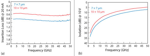
Figure 4 Insertion loss (a) and isolation (b) vs. frequency of single, shunt PIN diodes, comparing 7 x 7 and 10 x 10 µm diodes.
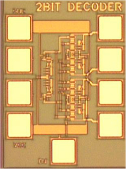
Figure 5 2-bit decoder logic function, one of several logic cells available in E/D PHEMT GaAs process.
ADDED FUNCTIONS
To meet the requirements of mmWave front-ends, the chosen process platform must provide excellent power and noise performance and have a low loss switch capability. However, that is not enough to provide a truly integrated front-end solution. To extend the feasibility of GaAs, several historic weaknesses of PHEMT technology must be addressed: adding multiple diode types for ESD protection, mixers and power detectors and standard logic cells and circuits for biasing and control interfaces.
The availability of on-chip logic is particularly important for active antenna arrays, as it simplifies the interface with the beamformer IC. A library of logic solutions, such as the 2-bit decoder shown in Figure 5, is available and continually expanding with more logic functions. These capabilities have been incorporated into the baseline PHEMT technology and are provided to the user as process options to meet application requirements. By adding libraries of logic cells and ESD reference circuits, GaAs technology offers users an entirely new toolset to support high performance mmWave front-ends.
In addition to functionality, the GaAs PHEMT platform must enable compact front-ends that fit within the 5 mm antenna spacing at 28 GHz or the 3.75 mm at 39 GHz. As excessive transmission losses at these frequencies are costly, the front-end components should be close to the antenna elements. The industry’s expectation is for the front-end MMICs to be attached directly to the antenna boards, which requires a chip scale package. To enable this assembly capability and minimize MMIC size, advanced platforms such as PIH1-10 incorporate a copper redistribution layer with copper pillar bumps. With the inherent humidity resistance of the technology, a chip scale, mmWave front-end can be realized.
SUMMARY
mmWave access points using active antenna arrays will play an important part in the development of 5G network services. As the industry adopts hybrid beamforming, designers will have more flexibility when choosing semiconductor technologies to meet specific use cases. Stringent performance specifications demand best-in-class semiconductor technology for front-end PAs and LNAs. Advanced and highly integrated GaAs PHEMT platforms will be a competitive technology to lower hardware costs and enable high performance, single chip, mmWave front-ends.

References
- T. Cameron, “RF Technology for 5G Millimeter Wave Radio,” www.analog.com/media/en/technical-documentation/white-papers/RF-Technology-for-the-5G-Millimeter-Wave-Radio.pdf.
- B. Peterson and D. Schnaufer, “5G Fixed Wireless Access Array and RF Front-End Trade-Offs,” Microwave Journal, www.microwavejournal.com/articles/29707.
- D. Corman, “All-Silicon Active Antennas for 5G/SATCOM Terminals,” Microwave Journal, www.microwavejournal.com/articles/29708.
- B. Sadhu et al., “A 28 GHz 32-Element Phased-Array Transceiver IC with Concurrent Dual Polarized Beams and 1.4 Degree Beam-Steering Resolution for 5G Communication,” 2017 IEEE ISSCC.