
With the roll-out of mmWave 5G expected to commence soon, the research and development activities of the industry’s key players are now well advanced and reached the point where custom components have been specified, designed and evaluated. An essential component required to enable future mmWave 5G systems is the front-end module (FEM) providing the final stages of amplification in a transmitter and the earliest stages of amplification in a receiver together with a transmit/receive (Tx/Rx) switch to allow time division duplex (TDD) operation. The FEM must demonstrate high linearity in transmit mode and low noise figure in receive mode. As mmWave 5G systems are likely to require user terminals containing multiple FEMs as part of a phased array or switched antenna beam architecture, they must also be highly efficient, compact and low cost. Ease of control and monitoring is also highly desirable.
This article describes the design, realization and evaluation of an FEM MMIC for the 28 GHz 5G band (27.5 to 28.35 GHz) which satisfies all of these requirements. The part was developed by Plextek RFI and designed on WIN Semiconductors’ PE-15 process which is a 4 V, 0.15 µm, enhancement mode GaAs PHEMT process. It is realised in a compact, low-cost 5 mm x 5 mm plastic overmolded SMT compatible QFN package making it suitable for high volume, low cost manufacture. It covers 27 to 29 GHz and so encompasses the full 28 GHz 5G band.
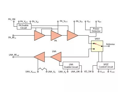
Figure 1 Block diagram of FEM MMIC for 28 GHz 5G.
Design Goals
The design of the FEM’s transmit path focused on achieving high efficiency when operating at back-off to provide linear amplification, as will be required by 5G systems. A target power added efficiency (PAE) of 6 percent at back-off was specified, with third-order intermodulation (IMD3) levels below ‐35 dBc (around 7 dB backed-off from the 1 dB compression point). The RF output power at the 1 dB compression point (P1dB) was specified at 20 dBm. For the receive path, a noise figure of below 4 dB (including switch losses) was required with very low current consumption—a target of 15 mA maximum from the +4 V supply was specified.
A block diagram depicting the functionality of the FEM MMIC is shown in Figure 1. The transmit signal path runs from left to right in the top half of the diagram; the input is at the pin labelled “PA_RFin.” The signal is amplified by a three-stage PA and then routed to the antenna via an RF power detector and a single pole double throw (SPDT) switch. The on-chip directional power detector allows monitoring of the transmitted RF output power and incorporates temperature compensation. The compensated detector output is given by the difference between the voltages “Vref” and “Vdet.” A fast switching enable circuit “PA Enable Circuit” is included on-chip and is controlled by the (active low) logic signal “PA_ON.” This is used to rapidly power up and power down the PA when switching between Tx and Rx mode such that it draws only 0.1 mA when not in use, maximizing the overall system efficiency.
The PA will typically operate backed-off from compression to preserve modulation fidelity of the transmitted signal. The design approach was to optimize the performance of the PA when operating 7 dB back-off from P1dB. In order to optimize PAE at this operating point the PA was biased in deep class AB.
Design Trade-offs
The design was initiated by running device level simulations on candidate unit cell transistors. This work forms a solid foundation for the subsequent detailed PA design as it yields key information such as device sizes, bias points, impedance targets, required number of PA stages and drive ratios.
A significant part of this work was aimed at identifying how to maximize PAE at back-off. Generally speaking, this is achieved by reducing the device quiescent bias current density. However, the extent to which this approach can be adopted is limited by the gain and linearity, both of which degrade as the current density is reduced. There is a clear trade-off of PAE (at back-off) with gain and linearity.
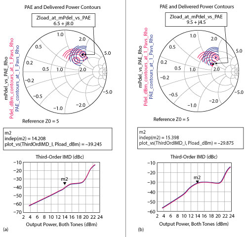
Figure 2 Load for optimum PAE at P1dB and corresponding IMD3 at back-off (a) and load for optimum power at P1dB and corresponding IMD3 at back-off (b).
The main linearity metric of interest was the IMD3 level at back-off which had to be below ‐35 dBc. It was found that the IMD3 performance at reduced bias currents became particularly sensitive to the fundamental load condition, as illustrated in Figure 2. Figure 2a shows load-pull simulation results for an 8 × 50 µm device biased toward deep class AB at 75 mA/mm at 4 V and highlights the optimum load for PAE at P1dB. It also shows the corresponding simulated IMD3 performance at back-off for this load and indicates that there is about 4 dB margin on the specification of ‐35 dBc. The simulated PAE at the same back-off was about 15 percent which is for the device only and excludes any output losses. Figure 2b shows similar information for the load condition that is best for power at P1dB. The IMD3 performance at the same relative back-off is considerably worse, more than 5 dB outside the specification, PAE at back-off was similar at around 15.7 percent.
Other points on the Smith Chart were also evaluated for performance at P1dB and at back-off, but the load condition, highlighted in Figure 2a, was found to be the best overall and was selected for the output stage design. This also offered scope for further bias current reduction, into deep class AB, to trade some IMD3 performance for PAE performance while still maintaining adequate gain. A bias current of 52 mA/mm was ultimately chosen and an 8 × 50 µm device selected as a suitable unit cell for the output stage, allowing the power specification to be met. It was also determined that three stages would be required to meet the overall transmit gain specification.
The design of the complete three-stage PA progressed with selection of the optimum transistor sizes for the driver and pre-driver stage. Again careful trade-offs were considered; larger transistor sizes improve the overall linearity but reduce the PAE. With the size and bias of all transistors selected the detailed design of the matching and biasing circuitry could proceed. The layout was considered from an early stage of the design process to ensure a practical implementation was possible without incurring unacceptable parasitics. A common gate bias line was used for stages one and two (applied at pin PA_Vg12) and a separate bias line for stage three (PA_Vg3). This allowed the possibility of separately optimizing the two voltages for potential linearity or PAE improvements to the PA. The drain supplies were similarly applied through two separate pins, although these were connected on the PCB; the +4 V drain supply is applied at “PA_Vd12” and “PA_Vd3.”