
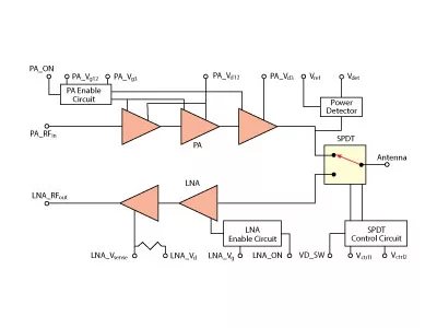
The SPDT switch is a series-shunt design incorporating multiple transistors in both the series and shunt arms for improved linearity.1 The off-state capacitance of the transistors limits the inherent isolation of the off-state device at high frequencies; at 28 GHz the switch transistors will have an isolation of just a few dB.2 Reducing the transistor size to improve the inherent isolation increases the on-state insertion loss and degrades its linearity and so was not an option. The approach taken was to include on-chip inductive compensation to improve the off-state isolation. Care was taken to ensure low insertion loss in the on-state to enable a high output power from the transmit path and a low noise figure from the receive path. The switch is controlled by a single bit, “Vctrl1,” which is set to 4 V for Tx mode or 0 V for Rx mode. Single bit control is facilitated by the “SPDT Control Circuit,” which is essentially a one to two line decoder. The combined supply current drawn by both the control circuit and the SPDT itself is just 1 mA from the +4 V applied at “VD_SW.”
The input to the receive path is at the “Antenna” pin which is routed to the input of a two-stage LNA by the SPDT. The output of the receive path is at the pin labeled “LNA_RFout.” As with the PA, the LNA also has a fast switching enable circuit such that the LNA draws as little as 0.1 mA when not in use. A key part of the LNA design process was to produce a design which had low current consumption but good noise figure and adequate linearity.
Selection of appropriate transistor sizes was an important first step. Multiple short fingers were used to reduce the gate resistance of the transistors and improve the noise figure. Series inductive feedback was added to both stages to shift the impedance required for optimum noise figure closer to that required for a conjugate match and optimum gain.
The first stage of the LNA was optimized for noise figure but still had to produce enough gain to adequately reduce the impact of the second stage noise figure. The noise figure of the second stage is not as critical, and this stage was designed with higher gain than the first. The resulting LNA design requires just 10 mA of DC supply current from its +4 V supply. The gate bias voltage is applied at pin “LNA_Vg” and the +4 V drain bias is applied at “LNA_Vd.” The “LNA_Vsense” pin is provided to allow for bias current monitoring. Monitoring the bias current allows control of the gate voltage to compensate for changes in environmental conditions, for example a change in temperature. When correctly biased this monitoring pin is at 3.9 V. The use of an enhancement mode process meant that only positive supply voltages were required, making the MMIC very convenient for system integration.
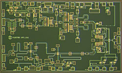
Figure 3 Die photograph of FEM MMIC for 28 GHz 5G.
Careful EM simulation was essential to ensure good RF performance from the various blocks. A step by step approach was adopted adding a part of the circuit to the EM simulation at a time with the rest of the block still simulated using Process Design Kit (PDK) models. As the IC was destined for packaging in an overmoulded plastic package, the presence of the moulding compound on top of the IC also needed to be accounted for in the EM simulation.
Evaluation and Test
A photograph of the FEM die is shown in Figure 3. The FEM MMIC die measures 3.38 mm × 1.99 mm. Its pad/pin positions are similar to those shown in the block diagram although it incorporates a number of GND pads in order to make it fully RF-on-wafer (RFOW) testable. It was designed to be packaged in a low-cost plastic overmolded5 mm × 5 mm QFN. In addition to accounting for the effects of the moulding compound, the RF transition from IC to PCB needed to be carefully designed. A custom lead-frame was designed to facilitate this and the RF ports of the package are all implemented as ground-signal-ground interfaces.
Following fabrication, several of the die were tested RFOW which confirmed that the first pass design had been successful prior to packaging. The RFOW results are not presented here but all measurements were made on a packaged assembled IC mounted on a representative evaluation PCB.
The evaluation PCB was designed using a low cost laminate PCB material suitable for mass volume production. Samples of the packaged FEMs were assembled on to the evaluation PCBs; all of the measured performance is calibrated to the package pins on the evaluation PCB and include the effects of the IC to PCB transition. A TRL calibration tile was designed to allow the calibration of the measured performance to the reference planes of the package. A photograph of one of the evaluation PCBs next to a TRL calibration PCB is shown in Figure 4.
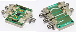
Figure 4 Photograph of packaged FEM evaluation PCB and TRL calibration PCB.
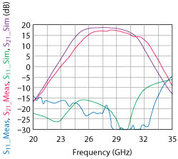
Figure 5 Measured to simulated small-signal performance of the Tx path of the FEM.
Evaluation results for the packaged FEM MMIC mounted on the PCB and referenced to the package’s RF pins. Throughout the evaluation, a commercially available multi-channel DAC and ADC IC was used to control and monitor the FEM. The FEM does not require any negative voltages as it was designed on an enhancement mode process. A comparison of the measured to simulated S-parameters of the Tx path of a typical FEM are shown in Figure 5. The measured data and simulated results match reasonably well. In this mode, the LNA is powered down, the SPDT control bit “Vctrl1” is toggled high and the PA biased to around 70 mA total quiescent current from +4 V. Small signal gain (S21) is 17.1 dB ± 0.4 dB from 27 to 29 GHz. The input return loss (S11) is better than 18 dB across the band. The output is matched for best PAE at back-off rather than best S22 but the measured S22 (not shown) is 8 dB or better across the band.
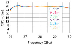
Figure 6 FEM Tx OIP3 vs. frequency vs. output tone power (100 MHz tone spacing).
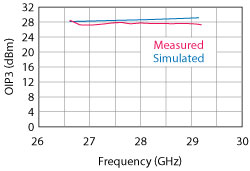
Figure 7 Comparison of measured and simulated OIP3 vs. frequency.
The output referred third-order intercept point (OIP3) of the Tx path was evaluated with a tone spacing of 100 MHz to reflect the wide channel bandwidths anticipated in 5G systems. Figure 6 is a plot of the measured OIP3 of a typical FEM with the wanted output tone powers ranging from 1 to 11 dBm per tone. It can be seen that the OIP3 is around +28 dBm across the 5G band and shows very little variation with tone power over a 10 dB dynamic range. A plot comparing the measured to simulated OIP3 versus frequency is shown in Figure 7 and demonstrates good agreement.