

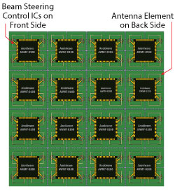
Figure 6 All-silicon architecture enables the RF front-end to be imbedded within the lattice of the array, i.e., on the backside of the antennas.
All-Silicon Array
The second active antenna architecture is an all-silicon array, where the beam steering control ICs reside within the lattice (see Figure 6). The beam steering control ICs contain the transmit output, receive input, gain control and phase control electronics, integrated on a single silicon die. The die may be transmit only, receive only or half duplex transmit/receive. Locating the die within the lattice of the array yields low feed loss between the die and the radiating element. With this planar construction, the control ICs are mounted on one side of a multilayer PCB, and the radiating elements are on the opposite side of the board. As shown in Figure 6, each control IC drives four radiating elements.
Advantages of this architecture include the lowest possible feed loss, which maximizes transmit EIRP and receive G/T efficiency. Since the individual radiating elements have unique amplitude and phase settings, this approach provides for full 2D scan, required for LEO/MEO SATCOM, mobile SATCOM and high density, urban applications. Another advantage of this architecture is using only high-yield silicon processes, the lowest cost processes in the industry, widely available from mainstream global suppliers. A typical silicon wafer size is 12 inches, which offers four times the wafer area compared to 6-inch GaAs and GaN. The high levels of integration available with silicon allow system on a chip (SoC) capability, where features can be imbedded to eliminate the need for array calibration. These are essential to meet the aggressive cost targets required by mass markets, such as mmWave SATCOM and 5G active antennas. Additional advantages of this architecture are
- silicon ICs can provide telemetry to the host system, which is useful for health and status reporting and scheduling preventative maintenance
- only a single power supply voltage is needed
- no DC sequencers are required, simplifying system cost and complexity.
Challenges with the all-silicon architecture are
- the number of ICs required per array is N/4, where N is the number of radiating elements in the array and each control IC drives four antenna elements
- transmit power per element is typically limited to +20 dBm, much lower than what is achievable with GaAs or GaN processes.
However, the need for more ICs with this architecture is more than offset by using the lowest cost semiconductor processes. The lower transmit power per element can also be compensated for by enlarging the array, taking advantage of the 20log(N) EIRP characteristic of transmit active antennas. Enlarging the transmit array is not necessarily “bad,” since a larger array allows lower transmit power per element, which spreads the heat over a larger area and helps the thermal design. By enlarging the array and using aperture gain to develop EIRP, rather than the RF power per element, reduces the overall DC power consumption of the array.
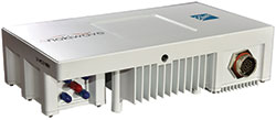
Figure 7 Anokiwave 256-element, all-silicon array.
Measured data on Anokiwave’s 256-element, all-silicon array (see Figure 7) validates the performance of the all-silicon array architecture. At 28 GHz, the array provides a G/T of ‐1.1 dB/K in receive and an EIRP of +59.7 dBmi in transmit. Comparing the measured results with theoretical calculations, the transmit EIRP is calculated from
EIRP = 20log(N) + Ge +
Powerelement – Losses
where N is the number of elements in the array, Ge is the imbedded element gain (+5 dBi for a λ/2 lattice), Powerelement is +8.5 dBm and losses total 1.5 dB for the combined feed loss, element ohmic loss and radome loss. The calculated EIRP is
EIRP = 20log(256) + 5 + 8.5 1.5 = 60.2 dBmi
which is within 0.5 dB of the measurement. Similarly, the receive G/T is calculated from
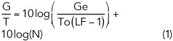
where N and Ge are the same as for the transmit array, To is the 290°K reference temperature, L is the sum of the front-end losses
(1.5 dB total or 1.41) and F is the noise factor of the receiver. Using 256 elements, +5 dBi imbedded element gain (3.14), 1.5 dB in losses and 5 dB NF (F = 3.16),
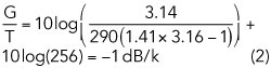
which closely agrees with the measured results for the array.