
Plastic-packaged FETs for High Power Applications
Amcom Communications Inc.
Clarksburg, MD
With the advent of wireless communications, demands have increased for high power, high linearity and inexpensive power amplifiers. Devices capable of handling high power along with high linearity are being used to design power amplifiers that achieve the high performance and reliability required in these applications. Using one high power device instead of combining several low power devices reduces combining losses and circuit board area, increases efficiency and reliability, and ultimately reduces design time and costs.
 Traditional high power FETs are housed in relatively expensive ceramic packages. A new family of unique GaAs MESFET devices have been developed that are housed in a low cost plastic package. The new TF series high frequency devices are inexpensive and feature high power and high linearity. One of the unique features of the FETs is that they are not prematched, thus the devices can be used for high frequency, wideband designs.
Typical Performance
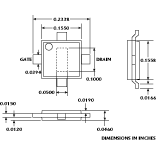
 A typical example of the TF family is the model AM144MX-TF GaAs MESFET designed for high power microwave applications up to 8 GHz with a total gate width of 14.4 mm. The new plastic-packaged device is supplied with straight pretinned copper leads in a drop-in mounting style. Two of the leads are the RF input and outputs; the other two are the grounding leads. The bottom of the package serves simultaneously as a DC and RF ground as well as a thermal path. The unique packaging provides three heat sink paths for effective heat removal. Figure 1 shows the package outline dimensions.
|
Table 1 | ||
|
|
Vds = 7 V |
Ids = 0.5 Ids |
|
P1dB (dBm) |
35.0 |
36.5 |
|
Efficiency at P1dB (%) |
26 |
40 |
|
Gain (small signal) (dB) |
11 |
13 |
|
IP3 (dBm) |
45 |
48 |
 The new device features a 36.5 dBm saturated output power at 2 GHz and high gain. Table 1 lists the AM144MX-TF device’s performance at 2 GHz and 25ºC. Typical saturation current Idss for the device at Vds = 3 V and Vgs = 0 is 3.4 A, and maximum pinch-off voltage at Vds = 3 V is -2.6 V. The device’s typical drain-to-gate breakdown voltage is 15 V and typical thermal resistance is 6.5ºC/W.
A Design Example
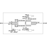
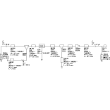
 A design example of a single-stage power amplifier using the model AM144MX-TF FET demonstrates the device’s performance capabilities. The output matching circuit is designed for optimum power output while the input matching circuit is designed to obtain maximum gain and input return loss. Figure 2 shows the circuit layout on a 20-mil board with a dielectric constant of 10.2, and Figure 3 shows a simplified
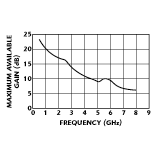
 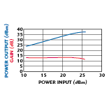 circuit diagram of the design. The device’s measured small-signal gain and return loss vs. frequency at Vdd = 7 V and Ids = 1.6 A are shown in Figure 4 . Figure 5 shows the output power and gain achieved at 1.4 GHz. The measured output power at the 1 dB compression point is 37.2 dBm and the power gain is more than 13 dB for a Vdd of 7 V and Ids of 1.6 A. Figure 6 shows the device’s maximum available gain as a function of frequency.
 Applications for the new plastic-packaged high power FET include wireless local loop and wireless local area networks, PCS base stations, repeaters, hyperLANs and very small aperture terminals. The new FETs significantly reduce the cost of high power devices in these applications without compromising performance.
Amcom Communications Inc., Clarksburg, MD (301) 353-8400.