
Today’s aerospace and defense (A&D) systems rely on semiconductors that address mission-critical availability, performance, processing and security requirements, while balancing demands for continuous size, weight and power (SWaP) reduction in each new generation of hardware. The GLOBALFOUNDRIES® (GF) FX-14™ ASIC design system merges advanced semiconductor technology with a unique combination of ASIC development methodology, tools, services and GF yield ownership to help A&D companies meet these demands and quickly bring ASICs from concept to production.
FX-14 is designed for next-generation communications and data center hardware, including digital baseband processing solutions for A&D command and control, radar and global positioning system applications. To meet the requirements of these applications, where both SWaP and frequency are crucial, FX-14 utilizes GF’s commercial 14 nm low power FinFET CMOS process technology, 14LPP.
SWaP-OPTIMIZED IP AND FEATURES
The FX-14 design system includes a library of silicon-proven IP:
- Multiple threshold voltage (Vt) FET options for managing power and performance
- Standard cell combinatorial gates, flip-flops and latches
- Phase-locked loops
- 64-bit and 32-bit ARM® processors
- A memory compiler that provides multiple embedded memory options (register arrays, register files, ROM, SRAMs and TCAM)
- An array of high speed SerDes (HSS) cores, including an advanced 56G offering.
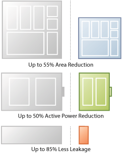
Figure 1 FX-14 SWaP benefits compared to GF Cu-32 ASIC process. Results will vary with design.
The inherent advantages of the 14LPP process technology and FinFET architecture enable significant SWaP benefits (see Figure 1). In addition, the FX-14 library features SWaP-centric elements that enable extensive design flexibility in optimizing solutions for the A&D industry. The embedded memory compiler takes advantage of multiple memory bit cell designs to meet design operational (row address/bit word, single/multiport), density (die area/size) and frequency requirements. An exceptionally small memory cell can be used to optimize memory density for applications requiring minimal die area, while a performance-tuned memory cell can help maximize memory performance (frequency) for performance-driven applications.
The variety of I/Os available with FX-14 provides additional SWaP benefits, useful for reducing ASIC I/O count, die size and power. I/O choices include:
- Three-state bidirectional CMOS I/Os
- Low voltage differential signaling (LVDS) I/Os
- Multiple HSS cores for both short and long reach communication
- LPDDR4 PHY
- A high bandwidth memory (HBM) Gen2 PHY, compliant with the JEDEC HBM2 standard and supporting data rates up to 2000 Mbps per data pin.
Features such as selective voltage binning and off-die switched voltage islands provide further opportunities for SWaP reduction. Voltage binning allows the ASIC supply voltage to be chosen according to the process speed, which is measured during ASIC manufacturing test and recorded within the die. Voltage islands can be used to power down circuits and IP when not in use.
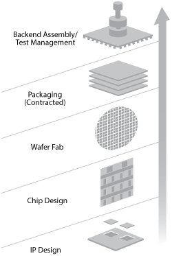
Figure 2 GF offers a vertically integrated, full service ASIC solution.
END-TO-END SOLUTION
GF pairs FX-14 silicon IP with a vertically integrated and validated ASIC development methodology, optimized through decades of development experience and a strong record of first-time-right designs for a full service ASIC solution (see Figure 2). This combination helps optimize customer development schedules and minimize expense risks.
The GF ASIC development methodology utilizes industry-standard design tools and a three-phase netlist signoff process (release-to-floorplanning, release-to-preliminary and release-to-layout) with highly structured entrance and exit milestones. GF is responsible for manufacturing test insertion, ASIC physical design and first-level ASIC package design. GF is also responsible for physical design checking (design rule checking and layout versus schematic), mask build, test generation, wafer manufacturing, ASIC wafer test, package manufacturing, die-package bond and assembly (module) and ASIC module test. Additional service options are available, including architecture services and detailed design services.
The GF FX-14 ASIC design system encompasses both FX-14 IP and development methodology, resulting in GF owning manufacturing yield. This further minimizes customer development risk. Customers purchase yielded FX-14 modules from GF: modules containing both die and packages that pass GF ASIC manufacturing tests.
GF’s FX-14 die/package estimation tool estimates both ASIC die content and dimensions, including package (module) dimensions, based on customer and GF inputs. The tool affords valuable insights for A&D customers that need to meet specific application SWaP requirements. Additionally, GF development tools for ASIC voltage planning/selection and early ASIC power analysis enable early power estimation and trade-off analysis to help minimize power consumption in power-sensitive applications.
As part of GF’s extensive commercial semiconductor portfolio, FX-14 builds on 30 years of ASIC expertise, more than a decade of A&D insights gained as a Trusted Foundry supplier and more than 2000 designs released to mask build. The high performance processing, density and power-efficient features of the FX-14 underlying 14LPP technology, combined with an extensive silicon IP portfolio, holistic ASIC methodology services and vertically integrated supply chain, are designed to enable GF FX-14 A&D customers to quickly develop differentiated solutions addressing next-generation challenges.
GLOBALFOUNDRIES
globalfoundries.com