
High Power, Low Cost Ceramic Quadrature Couplers
CirQon Technologies Corp.
Gurnee, IL
Many of today’s high power amplifiers for cellular and PCS base station use are assembled in a network composed of several medium power amplifier stages coupled with 90° quadrature hybrids or couplers. The quadrature couplers are preferred over Wilkinson splitters because they improve individual amplifier performance by shunting some of the mismatch reflections to the associated terminations, thus protecting the input of the subsequent amplifier stage.
Now amplifier designers have an alternative to using laminated construction for these quadrature couplers. Plated and bonded copper (PBC) on ceramic (Al2 O3 ) overcomes the traditional conductivity and power handling limitations of organic couplers. PBC couplers provide 50 to 100 percent more power handling ability with little or no increase in size and offer part-to-part consistency and tighter phase and amplitude balance at a lower cost. These new 3 dB 90° quadrature couplers are capable of handling up to 400 W of output power, whereas similar couplers based on organic technology only provide 60 to 200 W capability. Therefore, achieving more power using organic couplers requires a larger size and more expensive component.
The PBC Process
The microstrip process used to manufacture PBC couplers is far simpler than the stripline method employed for typical organic coupler circuits. Q-Clad® is a semi-additive copper plating process developed specifically for ceramic. It is similar to a conventional semi-additive printed circuit board manufacturing process, but with some significant adaptations to make it compatible with ceramic materials.
 The process begins with a laser-machined or green-punched ceramic substrate, typically 96 percent alumina. The ceramic substrate is activated and plated with a thin (25 microinch) layer of electroless copper, which provides electrical conductivity across the entire surface and through all vias. The electroless copper layer is not an adhesion layer since the copper-to-ceramic bond is created later in the process.
Next, the substrate is laminated with a dry film photoresist and the circuit pattern is photoimaged into the resist layer using conventional photolithography. The pattern is developed and the openings in the resist layer define the areas to be plated with thick electrolytic copper. When they go through the electrolytic plating bath, all of the noncircuit areas are still covered by the photoresist. This layer protects the underlying electroless copper from the plating solution while allowing the exposed areas of electroless copper to plate with electrolytic copper. The plating process continues until the thickness of the copper meets the requirements of the application (typically 0.001" to 0.003").
 The remaining photoresist is then stripped from the board, once again exposing the underlying electroless copper. The board is briefly etched to remove the exposed thin copper layer and isolate the remaining circuit traces. Since the electroless copper is very thin, the etch process can be accomplished very quickly without affecting the geometry of the thick copper traces.
Finally, the board is fired in a controlled atmosphere at a temperature over 1000°C. This firing process creates the bond between the copper and ceramic substrate. The final copper circuit may be protected from oxidation with an organic solderability perservative or precious metal plating.
 PBC Coupler Performance
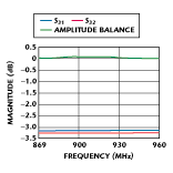
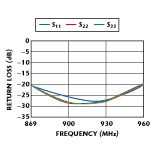
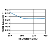
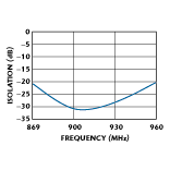
The Q-Clad PBC process results in a coupler that meets the demanding performance requirements of high power RF applications. The photoimaging assures precise line pattern definition to 75 mm, square side walls and good part-to-part repeatability in volume production. Trace shifting, which is common during production of organic substrates, is eliminated. Solderability of the PBC couplers is excellent due to the ceramic’s naturally hard, secure surface. Unlike organic couplers, the ceramic base allows heat to conduct out of the device while the copper traces remain cool. PBC couplers are currently available for cellular and PCS applications; both are capable of handling 400 W of power. Table 1 lists the couplers’ performance specifications. Figures 1 through 4 show performance vs. frequency for the cellular version.
 Applications
The PBC quadrature couplers have been specifically designed for applications in wireless base stations and equipment. They may be used as surface-mount components on a power amplifier mother board to combine the outputs of two or more power transistors where the power of each transistor is 50 W or greater. They also may be used to combine the outputs of two power amplifiers where the individual amplifiers have outputs up to 200 W each. Since the components are ceramic in construction, their operating temperature limits are very high. Ceramic has a much better thermal conductivity than organic materials (approximately 26 W/mK at room temperature). Ceramic is also dimensionally stable with temperature variations and does not absorb moisture. Thus, the couplers’ performance over environmental extremes is good.
|
Table 1 | ||
|
|
Cellular |
PCS |
|
Frequency (MHz) |
869 to 894 |
1930 to 1990 |
|
Insertion loss (dB) |
0.3 |
0.3 |
|
SWR (max) |
1.25 |
1.25 |
|
Amplitude balance (dB) |
0.2 |
0.2 |
|
Phase balance (°) |
2 |
2 |
|
Isolation (dB) |
20 |
20 |
|
Power handling (W) |
400 |
400 |
Conclusion
Cellular and PCS ceramic quadrature couplers have been developed using a PBC process that offers 50 to 100 percent more power handling capability with little or no increase in size and at a lower cost. In addition, the components feature tighter phase and amplitude balance and superior unit-to-unit consistency.
CirQon Technologies Corp.
Gurnee, IL
(847) 360-1900