
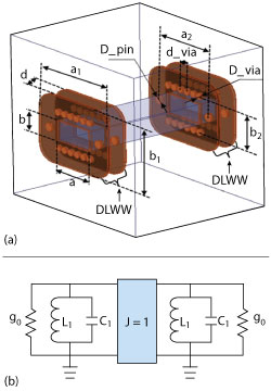
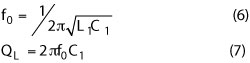
Figure 1 Back-to-back DLWW structure (a) and equivalent model (b).
A millimeter wave (mmWave) waveguide window employs a direct coupled filter network, which includes LC resonators and J inverters. ABCD matrix theory and full-wave simulation are used in the design. It is wideband and low-cost. Back-to-back waveguide sealed windows are built and measured. In the frequency range of 75 to 100 GHz, return loss is greater than 15 dB, insertion loss is less than 0.7 dB and the leakage rate is lower than 8×10⁻⁸ Pa.m3/s.
Millimeter wave components, usually constructed with waveguide interfaces, are widely used in millimeter wave systems. In order to improve reliability, the waveguide interfaces are sealed. There are several types of waveguide sealed windows frequently in use. One is a pillbox;1-5 however, detailed synthesis methods are not provided.1,2,4 Liu3 employs an ABCD matrix method for design, but the pillbox requires a complex welding process. Another is a resonance type,6,7 but its bandwidth is limited. Further approaches, such as multilayer waveguide windows,8 need different dielectric windows with different thicknesses that increase insertion loss.
In this article, a new double-layer waveguide window (DLWW) for mmWave components is designed to improve reliability while reducing cost. In addition, the bandwidth of the sealed window is increased relative to other designs. This design is carried out for W-Band back-to-back waveguide sealed windows by employing a direct coupled filter network design method using ABCD matrices and full-wave simulation.
SYNTHESIS AND FULL-WAVE SIMULATION
DLWW Circuit Description
The back-to-back waveguide sealed windows (see Figure 1) are designed using a broadband direct coupled filter synthesis method.9-11 Each DLWW is composed of two RT/Duroid 5880 substrates (thickness = 0.127 mm, εr = 2.2) and one quarter-wavelength waveguide (between the two substrates). The direct coupled filter model (see Figure 1b) is used for this design. The substrate is equivalent to a dielectric resonator (composed of C1 and L1), whose resonant frequency is determined by the parameters of substrate. The quarter-wavelength waveguides, which determine the coupling coefficient are equivalent to an admittance inverter of value J = 1.
DLWW Synthesis
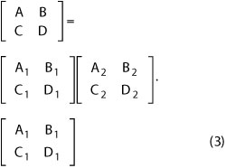
The ABCD matrix and scattering parameters are used to determine the DLWW parameters. According to Figure 1, the two-port matrix of the dielectric resonator is
and the two-port matrix of the quarter-wavelength waveguide is
where ι is the length of quarter-wavelength waveguide, and ß is the propagation constant.
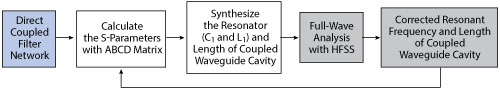
Figure 2 Waveguide window synthesis procedure.
The cascaded dual-port ABCD matrix of the DLWWs is
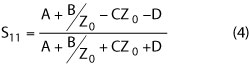
The input return loss (S11) of the DLWW is expressed as
Therefore, the transmission power ratio is
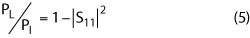
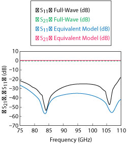
Figure 3 DLWW model vs. simulation.
where PL is the power delivered to the load and PI is the available power from the source.
As shown in Figure 1b, this model provides the parameters of the network, namely, the resonant frequency (f0) and the loaded quality factors (QL) of each dielectric resonator.
The dielectric resonator’s f0 and QL can also be deduced from its scattering parameters through full-wave simulation.11
where Y11 is the input admittance of the dielectric resonator.
The synthesis procedure for the DLWW is shown in Figure 2. First, the direct coupled filter model is used to synthesize the DLWW. Then, the scattering parameters are derived using its ABCD matrix. Third, the dielectric resonator’s (f0,QL) and the length of coupled waveguide cavity are determined when S11 reaches a minimum. The full-wave model is then established and simulated. Finally, the direct coupled filter network parameters are corrected through full-wave simulation.
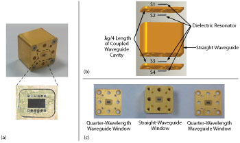
Figure 4 Photo (a) and exploded view (b) of back-to-back waveguide windows. Exploded view of welded quarter-wavelength waveguides and straight waveguide (c).
DLWW Full-Wave Simulation
The Ansoft HFSS full-wave simulator is used to accurately calculate the size of the dielectric resonator and the coupling cavity. The design parameters are defined in Figure 1a and their numerical values are: a = 2.54 mm, b = 1.27 mm, a1 = 5.54 mm, b1 = 4.27 mm, a2 = 4 mm, b2 = 2.26 mm, d = 0.86 mm, d_via = 0.508 mm, D_via = 0.4 mm and D_pin = 0.5 mm. Figure 3 shows predictions from the equivalent model and the full-wave simulation. The full-wave simulation takes into account the loss of the transmission medium, so the curves are not exactly the same. From 75 to 108 GHz, the return loss is greater than 20 dB for the full-wave simulation curves.
FABRICATION AND TEST
Window Fabrication
The fabricated waveguide windows are composed of two DLWWs and one 15 mm length of straight waveguide (see Figure 4a). The dielectric resonators are fabricated using a PCB process with RT/Duroid 5880, giving the DLWWs the advantages of low complexity and low-cost in manufacturing. The waveguide is gold-plated aluminum alloy. The flange of the waveguide is WR10.
As shown in Figures 4b and 4c, dielectric resonators S2 and S3 are welded onto the straight waveguide, and dielectric resonators S1 and S4 are welded onto the quarter-wavelength waveguides for the sealing. The solder is Au-Sn with a thickness of 0.025 mm. The welding temperature is 280°C. Two quarter-wavelength waveguide windows and one straight waveguide window are assembled with screws to form the back-to-back waveguide window (see Figure 5).
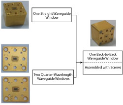
Figure 5 Back-to-back waveguide assembly.
Test Results
To accurately test performance, a straight waveguide (length of 15 mm) is designed. Figure 6 shows measured scattering parameters compared with simulated results using Ansoft HFSS. Simulated return loss is higher than 20 dB and insertion loss lower than 0.2 dB in the frequency range of 75 to 100 GHz. Measured return loss is higher than 15 dB and measured insertion loss (after deducting the straight waveguide insertion loss) is better than 0.7 dB from 75 to 105 GHz. The leakage rate measured on several back-to-back devices, using a helium spectrometer leak tester, is less than 8×10⁻⁸ Pa.m3/s.
CONCLUSION
A novel waveguide window for millimeter-wave module sealing is demonstrated. Its development was motivated by the desire for low complexity and low-cost in manufacturing. The structure is wideband compared with the resonance type windows. Measured results show that its return loss is greater than 15 dB and its insertion loss is less than 0.7 dB from 75 to 100 GHz for the back-to-back windows. The leakage rate is less than 8×10⁻⁸ Pa.m3/s.
ACKNOWLEDGMENTS
This work was supported by the National Natural Science Foundation of China (Grant No. 61101065).
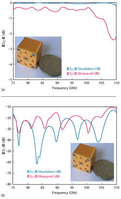
Figure 6 Simulated and measured S-parameters of back-to-back waveguide windows, |S21| (a) and |S11| (b).
References
- A. Srivastava, O. J. Kwon , M. Sattorov, A. Sharma, A. Tanwar and G. S. Park, “Broadband THz Vacuum Window Using Impedance Matching Approach,” 35th International Conference on Infrared Millimeter and Terahertz Waves, September 2010, pp. 1.
- I. Freidovich, B. Prokofiev, A. Balabanov, A. Yegorov, A. Zakirov and A. Grigoriev, “Waveguide Window for a Broadband Multibeam Ka-Band Klystron,” IEEE 14th International Vacuum Electronics Conference, May 2013, pp. 1–2.
- S. Liu, “A RF Window for Broadband Millimeter Wave Tubes,” International Journal of Infrared and Millimeter Waves, Vol. 17, No. 1, January 1996, pp. 121–126.
- L. Earley, E. Smirnova and P. Ferguson, “Experimental Measurements and Field Modeling for a W-Band Window,” IEEE 5th International Vacuum Electronics Conference, April 2004, pp. 244–245.
- A. M. Cook, C. D. Joye, T. Kimura, E. L. Wright and J. P. Calame, “Broadband 220-GHz Vacuum Window for a Traveling-Wave Tube Amplifier,” IEEE Transactions on Electron Devices, Vol. 60, No. 3, February 2013, pp. 1257–1259.
- M. E. Hill, R. S. Callin and D. H. Whittum, “High-Power Vacuum Window in WR10,” IEEE Transactions on Microwave Theory and Techniques, Vol. 49, No. 5, May 2001, pp. 994–995.
- S. Bashaiah, P. K. Sharma and K. C. J. Raju, “Fabrication of High Dielectric Constant and Low Loss X-Band Ceramic Waveguide Window for High Power Applications,” 5th International Conference on Computers and Devices for Communication, December 2012, pp. 1–4.
- M. C. Lin, “A Multilayer Waveguide Window for Wide-Bandwidth Millimeter Wave Tubes,” International Journal of Infrared and Millimeter Waves, Vol. 28, No. 5, May 2007, pp. 355–362.
- S. B. Cohn, “Direct Coupled Resonator Filters,” Proceedings of the IRE, Vol. 45, No. 2, February 1957, pp. 187–196.
- R. Levy, “Theory of Direct-Coupled-Cavity Filters,” IEEE Transactions on Microwave Theory and Techniques, Vol. 15, No. 6, June 1967, pp. 34–348.
- R. M. Barrio-Garrido, S. LIorente-Romano, A. Garcia-Lamperez and M. Salazar-Palma, “Design of Broadband Directly Coupled Non-Centred Resonant Irises Filters,” 33rd European Microwave Conferen