
The use of fast real-time oscilloscopes allows the recording of single transient events at GHz frequencies in the large signal operation of electronic components. With sampling rates over 100 GS/s, such equipment can be used to detect and store high frequency signals over a wide frequency spectrum. Sampling oscilloscopes that have been used for many years are restricted to periodic signals, e.g., with active harmonic pull. This article describes how real-time oscilloscopes can be used to capture single transient events that occur during device failure.
Standard measurement equipment such as network analyzers and spectrum analyzers are unable to record single transients. This limitation does not apply to the approach described here, making it particularly suitable for measuring non-periodic events. Not only RF behavior, but bias parameters as well, are recorded simultaneously. This places strict requirements on calibration of both the RF and bias circuits. Because there is no second source at the output, only the input reflection coefficient (S11) and forward gain (S21) are determined.
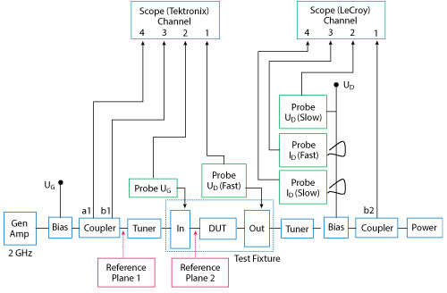
Figure 1 Measurement setup.
Most related measurement approaches determine breakdown under dc and pulsed dc conditions.1-4 Other measurement setups use load line analysis.5,6 All use sequential sampling techniques and thus require periodic signals. In this article, however, real-time sampling is used, allowing one-shot measurements essential for studying irreversible effects.
MEASUREMENT SETUP
The measurement setup resembles a classic load-pull system (see Figure 1). A generator and power amplifier provide the necessary RF-input power. A test fixture with input and output boards allows easy assembly and pre-matching of the device under test (DUT) while tuners provide matching to the 50 Ω environment. In this case the transformer pre-matches 22.5 to 50 Ω. The 22.5 Ω characteristic impedance is related to the transmission-line structure formed by the leads of the transistor package. DC power is provided through bias-tees. The scattering parameters are determined by means of directional couplers.
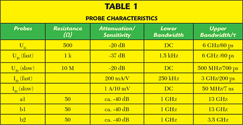
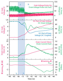
Figure 2 High time resolution measurements.
The load-pull setup is extended by real-time oscilloscopes with several measurement channels. A TDS 6124C by Tektronix and a WP 735Zi by LeCroy provide 8 measurement channels with 20 GS/s each for data recording. The analogue bandwidths are 12 GHz (Tektronix) and 3.5 GHz (LeCroy), respectively. Maximum memory depths of 8 M points/Channel allows a recording time of 400 µs in 50 ps steps. This makes the digital recording of the incident (a1), reflected (b1) and transmitted (b2) waves from the directional couplers possible. Relevant bias current and voltages are recorded as a function of time via the other oscilloscope measurement channels.
Voltage probes at the input and output boards measure gate and drain voltages while output drain current is measured with current probes. Because the fast drain voltage and current probes have lower cut-off frequencies, they are augmented with slower DC-coupled probes to record DC levels. The fast probes are bandwidth limited on the high end as well. A step of the drain voltage detected through the fast probe yields a signal at the oscilloscope that rises with a time constant at the upper bandwidth limit and then falls with the much slower time constant of the lower bandwidth limit. Table 1 shows the bandwidth limits of the relevant probes.
With regard to the transition ranges, input voltage and output currents and voltages may be measured over a wide time interval, ranging from picoseconds to seconds — enabled by the instruments’ large memory depths. Numerous trigger options allow triggering of many events. In this case, the trigger is activated by the lack of an output signal, i.e., the malfunction of the device under test. Using special features in the oscilloscopes, even events before the trigger are recorded and stored. Hence, it is also possible to look at the time prior to the malfunction; then, the trigger event simply ends permanent signal recording. The trigger-out signal of the faster Tektronix oscilloscope is connected with the trigger-in of the second oscilloscope. This is triggered after a very short, precisely-defined time delay.
CALIBRATION
In order to allocate the data to a timeline, it is necessary to first calibrate each system (load-pull as well as probes) individually. Then, both systems are adjusted to each other.
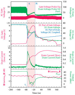
Figure 3 Medium time resolution measurements.
For this purpose, voltage probes on the input and output boards are placed directly at the location of the device under test (i.e., Reference Plane 2 in Figure 1) and a signal with a fast slope (e.g., a step function) is applied at Reference Plane 1. Channels 1 and 2 (voltage probe input and output) are calibrated for 0 ps delay to the leading transient of the input signal by adjusting the skew for each channel individually. Probe attenuation factors are determined separately using a calibrated signal generator output with a matched 50 Ω line.
Loading of the DUT by the probes must also be considered. The power transistors used here have low input and output impedances. Hence, the loading by the (nominal) real parts of the voltage probes of 500 Ω or 1 kΩ, respectively, is marginal. The capacitive part of the voltage probe input impedance, however, must be taken into account when setting up the matching boards and performing through-calibration of the load-pull system. Hence, the capacitive part is considered when determining the optimal source and load impedances through load-pull.
To determine the complex Gamma, a calibration at Reference Plane 1 with open, short and load is performed. With known S-parameters of the tuners and test fixture boards one can transform the reflection coefficient from Reference Plane 1, in the direction of the DUT, to Reference Plane 2.
TRANSISTOR MEASUREMENT
To demonstrate the performance and capabilities of the system, single-shot measurements of a gallium nitride (GaN) transistor with 10 mm gate width are conducted at a fundamental frequency of 2 GHz. The purpose of these measurements is to examine the behavior of the transistor during failure, when the drain bias voltage is increased step-by-step while keeping RF power constant.
The transistor is biased with a DC-power supply via bias tees. The DC bias point is set at a relatively low drain voltage (i.e., 28 V). Considering the influence of the probes, the optimum source and load impedances are determined by load-pull measurements. Load-pull tuning is conducted only at 28 V in order to avoid the risk of transistor failure, because the tuning procedure takes it outside its safe operating area at higher drain voltages.
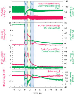
Figure 4 Low time resolution measurements.
The transistor is then driven to its P1dB point by applying the relevant source and load impedances derived under 28 V bias. Next, the drain voltage is increased step-by-step, while keeping all other conditions including the RF input power unchanged. At a certain drain voltage, the transistor will fail. The Tektronix oscilloscope triggers the failure of the RF-voltage and stops all other measurements.7 This is independent of the reason for failure, which may be high drain voltage, high drain current or high dissipated power. With data stored for the time prior to malfunction, the failure mechanism can be investigated in detail.
MEASUREMENT RESULTS
Using the calibration routine described earlier, the measurement data stored in the memories of each channel is allocated to a timeline. The high memory depth of the oscilloscopes in single shot mode allows a good overview as well as the possibility to examine all details within the maximum sample rate of 20 GS/s. Figures 2 through 4 show the transistor parameters obtained in this way for different time scales. Analyzing this data one finds that the breakdown process occurs in four phases:
Phase I: The first changes appear at point t0 = -80 ns (trigger offset). The drain voltage decreases while drain current and gate voltage increase. The output power still remains constant. It is probable that a drain-gate breakdown has occurred. The leakage current from drain to gate shifts the bias point (see Figure 5a).
Phase II: At time t1 a further drain-gate breakdown takes place forming a low-impedance connection between the drain and gate. The gate voltage becomes significantly positive and the drain current increases rapidly. Now, the output power and drain voltage drop continuously. There is an overshoot at the slow drain voltage probe due to the probe inductance. The RF output power reaches its minimum.
The end of Phase II is denoted by t2 when the gate voltage reaches a maximum at +6 V. The drain current reaches a temporary maximum as well at t2. This may be the point when the air bridge at the drain of the respective finger bends because of the high current density there (see Figure 5b). Note that air bridges are more vulnerable to high current densities since they are missing the heat sinking through the substrate. This bending brings the air bridge in close proximity to the metallization below and thus initiates a local breakdown.
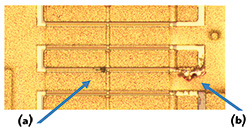
Figure 5 Photograph of the damaged transistor, showing damage in the gate area (a) and at the drain air bridge (b).
The resulting high current causes a protection fuse to switch off the drain power supply. Now, the remaining current results from discharging of capacitance in the drain bias circuit.
Phase III: Due to the short circuit at the drain, the drain current increases, the drain voltage drops and the gate voltage returns to its default value because no current flows from drain to gate. As a consequence, the air bridge cools down and reopens the drain-source contact.
Phase IV: Since the drain contact is open, the gate voltage increases rapidly again, but not to the high values at the beginning because the power supply is switched off and the drain voltage relates to the remaining charge in the bias capacitors. The effect is not seen at the drain probe because of probe inductances.
This repeats for some time until the bias circuit capacitors are empty of charge. At the end, the air bridge melts and there is a permanent short at the drain air bridge and a short between gate and drain (and source) as a result of the breakdown. During the entire time after the failure, change of the input reflection coefficient is monitored. It is assumed to be caused mainly by variations of the other operational parameters during the failure process.
Figure 6 shows the trend of the complex input impedance during transistor failure within a Cartesian coordinate system. The change of the reactive part from 4 to 4.5 Ω with 6 Ω in the interim is particularly remarkable. Clearly, the impedance changes in discrete steps. Presumably some parts of the gate fail which leads to a gradual decrease of the input capacitance. Note that the input capacitance of a working transistor is higher because of the Miller capacitance and it decreases when gain is reduced. Thus, the input capacitance of the damaged transistor is lower than before. After the damage, small parts of the gate structure are no longer operational and short circuit the entire transistor.
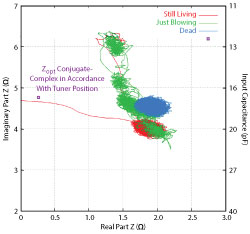
Figure 6 Trend of the complex input impedance during transistor failure.
Measurements and photographs reveal the following picture for the possible course of destruction of the transistor: Due to high field strength and overheating, a drain-gate breakdown occurs starting from t0 onwards. The high current flow in turn causes a high current density within the corresponding drain air bridge. These air bridges are not sufficiently cooled by the substrate, become overloaded by the current, bend and in turn cause a short circuit. This short circuit reopens if temperature decreases and so an oscillation of drain shorting may occur. It is presumably the combination of the overheating of the transistor and the high drain field strength that leads, finally, to transistor destruction.
CONCLUSION
The measurement setup described allows characterization of linear and non-linear DUTs with periodic and single transient events, up to a fundamental frequency range of 4 GHz. Its special feature is the detection of single transient events, also irreversible ones as encountered, for example, during device failure. The system collects time-dependent data of bias as well as RF quantities, including S-parameters.
Its potential is demonstrated by investigating the failure mechanisms in a high-power GaN microwave transistor. In this way, conclusions regarding possible failure mechanisms can be drawn to assist in optimizing the devices and improving reliability. For example, it is found that care must be taken in designing the periphery such that all air bridges have a sufficient heat sinking to avoid thermal overload under all operating conditions.
One should note that the approach presented is not limited to the 4 GHz range used in our experiments. Oscilloscopes with bandwidths of up to 60 GHz and sample rates of up to 160 GS/s are state of the art. With the newest equipment, the approach described above could be extended to cover the 10 to 20 GHz range. Moreover, ongoing developments in the field of real-time oscilloscopes will enable further improvements in capability using this technique.
References
- B. D. Huebschman, A. Darwish, N. Goldsman, E. A. Vivieros and A. Hung, “Investigation of Breakdown Behavior for AlGaN HEMTs,” International Semiconductor Device Research Symposium, December 2009, pp. 1–2.
- E. Bahat-Treidel, F. Brunner, O. Hilt, E. Cho, J. Wurfl and G. Trankle, “AlGaN/GaN/GaN: C Back-Barrier HFETs With Breakdown Voltage of Over 1 kV and Low,” IEEE Transactions on Electron Devices, Vol. 57, No. 11, November 2010, pp. 3050–3058.
- M. Wang and K. J. Chen, “Off-State Breakdown Characterization in AlGaN/GaN HEMT Using Drain Injection Technique,” IEEE Transactions on Electron Devices, Vol. 57, No. 7, July 2010, pp. 1492–1496.
- C. –S. Suh, Y. Dora, N. Fichtenbaum, L. McCarthy, S. Keller and U. K. Mishra, “High-Breakdown Enhancement-Mode AlGaN/GaN HEMTs with Integrated Slant Field-Plate,” International Electron Devices Meeting, December 2006, pp. 1–3.
- W. McGenn, J. Powell, M. Uren, J. Benedikt and P. J. Tasker, “RF Waveform Method for the Determination of the Safe Operating Area of GaN HFET’s for Amplifiers Subjected to High Output VSWR,” European Microwave Integrated Circuits Conference, September 2010, pp. 282–285.
- M. Demmler, P. J. Tasker and M. Schlechtweg, “A Vector Corrected High Power On-Wafer Measurement System with a Frequency Range for Higher Harmonics up to 40 GHz” 24thEuropean Microwave Conference, September 1994, pp. 1367–1372.
- “TDS6000B & TDS6000C Series Technical Reference – Digital Storage Oscilloscopes Specifications and Performance Verification Technical Reference,” Tektronix, October 2006.

Armin Liero received his Dipl.-Ing. degree in communication engineering from the Technische Universität Ilmenau, Germany, in 1979. From 1979 to 1989, he was with the Academy of Science of the GDR, where he was responsible for design and development of the microwave part of Electron Paramagnetic Resonance Spectrometers. After 1989, he spent six years in different companies working on the development of high-speed digital oscilloscopes and microwave components. In 1995, he joined the Max-Born-Institut, Berlin, and was responsible for the RF part of synchronization of LASERS (MBI) and Linear Accelerators (DESY Hamburg). He has been with the Ferdinand-Braun-Institut, Leibniz-Institut für Höchstfrequenztechnik, Berlin since 2002. His current work is focused on microwave design techniques, packaging and development of high-current, short pulse LASER drivers.

Silvio Kühn received his university degree in computer engineering 2006 and his Ph.D. in the field of microwave induced plasma excitation in 2012. He has been with Phasor Instruments since 2013. His interests are network analysis and power electronics.

Olof Bengtsson received his Ph.D. degree from the Department of Solid State Electronics (SSE), Ångström Laboratory, Uppsala University, Sweden, in 2008. He was co-founder and managing director for the private limited company, Swedish Linear Microwave AB from 2002 to 2010. Since April 2009 he has been with the Ferdinand-Braun-Institut (FBH), Berlin, Germany, where he currently holds the positions head of the RF Power Lab and group leader for microwave measurements. His main interests are large-signal device characterization and high efficient RF power amplifier designs based on load and supply modulation.

Wolfgang Heinrich received his Ph.D., and habilitation degrees from the Technical University of Darmstadt, Germany. He has been with the Ferdinand-Braun-Institut (FBH) at Berlin, Germany, since 1993, as head of the microwave department and deputy director of the institute. He has also been a professor at the Technical University of Berlin since 2008. His present research activities focus on MMIC design with emphasis on GaN power amplifiers, mmWave integrated circuits and electromagnetic simulation.