
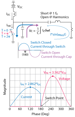
Figure 1 Standard Class E topology. With this type of circuit, duty cycle is an important design parameter to ensure reliable operation, as current and voltage swings can push device limits.
Power amplifiers (PA) are increasingly part of everyday life, used in everything from wireless and broadcast transmitters to hi-fi audio equipment. Due to its very high efficiency, the Class E PA topology is particularly advantageous for wireless communication devices. Unfortunately, that benefit comes at a price: a Class E PA circuit is difficult to design. It involves a number of design challenges and trade-offs that must be well understood in order to achieve a successful circuit implementation. Fortunately, a novel synthesis-based design process now promises to make designing a Class E PA faster and easier than before.
Class E Theory
Before designing a Class E PA, it is critical to understand the basic theory behind the topology. As opposed to the conventional classes of operation, Class E amplifiers use a transistor like a switch that toggles on and off at the fundamental frequency (see Figure 1). A series resonator added to the output acts like a short at the fundamental frequency and an open at the harmonics. This forces a single frequency (sinusoidal) current to flow through the circuit. When the switch is closed, AC current flows out of the resonator into the switch with the DC current from the supply. When the switch is open, current flows back into the resonator from ground through a capacitor. The voltage across the capacitor is the integral of the current.
If designed correctly, this switching mode circuit has the potential to be 100 percent efficient. The challenge, however, is that the voltage and current swings can be high multiples of the DC supply values. For example, when the switch toggles at the halfway point (50 percent duty cycle), the voltage peaks are several times that of the supply voltage. These swings can cause the signals to exceed the safe operating limits of the transistor, and this has significant implications for reliability.
Designers want to avoid such swings; therefore, successful circuit design requires using equations that vary with duty cycle. Unfortunately, enumerating these equations is not easy. Circuit design equations that include duty cycle are not compact, meaning that the resulting values are usually expressed in graphical format or in the form of a polynomial fit. Designers often have to interpolate normalized values from these graphs manually, and that can jeopardize the accuracy of the design.
Load-pull Simulation and a Lot of Patience
In general, PAs are designed using load-pull simulation. This technique involves sweeping the output load over a set of impedances, generating various contours for power and efficiency and picking the load value that gives the needed performance. Unfortunately, load-pull simulation doesn’t work well with a complex switching mode amplifier, like Class E.
In Class E, performance depends on presenting a very precise combination of fundamental and harmonic impedances to the intrinsic node of the device, along with an input signal drive level and bias point combination which set the switching duty cycle. To find such a specific combination of points using a brute-force technique like load-pull would require generating and sorting a huge volume of data. Even if it is feasible to take all the points, there would be no guarantee that the simulation would converge or remain stable over every possible combination of bias and impedance. There could be conditions where the model isn’t intended to be used because the device is intrinsically unstable or the simulation just doesn’t converge, which can result in interpolation errors. If designers arbitrarily follow this approach and rely too much on the device model without understanding circuit fundamentals, the results can be quite confusing and the device might even be damaged. For Class E, a more meticulous approach to the initial PA design is needed.
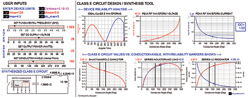
Figure 2 The Keysight ADS Class E power amplifier synthesis utility 2 generates Class E voltage and current waveforms across a transistor and analyzes these vs. reliability constraints.
New Synthesis-Based Approach
How can a Class E PA circuit be accurately designed without having to use load-pull simulation or manually interpolate plots of normalized equations? The key is an interactive circuit synthesis design process that relies on first principles to get an accurate prediction of the performance of an amplifier entirely from a starting set of equations and rules. This process enables PA designers to more quickly arrive at a predictable and understandable starting point.
The first step is to synthesize the circuit entirely from transient equations.1 Second, the circuit is validated using an idealized switch/lumped circuit topology. Third, the voltage/current waveforms are converted from the time domain to a set of harmonic impedances in the frequency domain. Finally, design tools are used to optimize a more practical, realizable circuit topology to match the target impedance values for the first few harmonics.
Key to this approach is the choice of synthesis tool (see Figure 2). Ideally, it should have a utility that allows the general Class E design equations to be encoded in an interactive manner so that circuit synthesis occurs in real-time based on design inputs. With this type of utility, the designer can enter the device parameters on the display (e.g., maximum voltage and current, knee voltage and the internal parasitic capacitance of the device) and set performance specifications (e.g., frequency, DC supply voltage, output power and conduction angle). The synthesis tool then uses this information to synthesize the ideal Class E circuit.
This type of synthesis tool offers the ability to plot circuit values against conduction angle and denote, with markers, the valid range under which the PA circuit can reliably operate. The conduction angles between the markers are valid, those outside the markers are not. When operation with any conduction angle is not possible, the designer is notified with a warning message. Such design flexibility is critical to ensuring the device operates reliably while meeting target performance specifications in the Class E circuit.
To see how this four-step process works, consider the example of a Class E PA design using a Cree GaN MMIC device and Keysight Advanced Design System (ADS) for synthesis. The device has a breakdown voltage of 120 V, an intrinsic capacitor value of 2.1 pF and a maximum AC and DC current of 4.5 and 3 A, respectively. The Cree model also allows access to the intrinsic current generator of the device, which is important because the target impedances achieved through the synthesis process must be presented across this node.
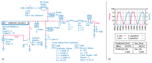
Figure 3 Ideal Class E circuit (a) and validation of the synthesized circuit (b). The solid lines in the graph are the simulation, while the dotted lines are predicted from the synthesis equations. This idealized large-signal simulation achieves about 99.9 percent efficiency.
Step 1: Synthesize the circuit from transient equations.
To generate the design, the device’s reliability limits and intrinsic capacitance are entered into ADS. The tool’s sliders are then used to set the frequency to 1 GHz, the supply voltage to 28 V and the output power to 25 W. The tool outputs a range of conduction angles that can be used for the design. In this case, the valid conduction angles range from 120° to 170°. If the conduction angle goes below 120°, the RF current will exceed device limitations; if the conduction angle goes above 170°, the required value of shunt capacitor is smaller than the intrinsic device parasitic. The interactive nature of this process provides a more complete understanding of the tradeoffs and limitations involved, helping to avoid errors later. Selecting a conduction angle of 160°, an ideal Class E circuit is obtained as shown in Figure 3.
Step 2: Validate the circuit using an idealized switch/lumped circuit topology.
The goal of the validation is to match the AC voltage and current waveforms, power and DC current, so that the circuit can be tried with the GaN device. It’s a good idea to validate in an ideal environment before moving to implementation using a real transistor. In this case, the circuit is validated using a simple simulation bench. The transistor is modeled using a switch component, the circuit values are brought in from the synthesis tool and a harmonic balance simulation is run. Figure 3 shows that the simulation results agree very well with the predicted waveforms. This level of agreement with simulated results is typical for the synthesis tool.
Step 3: Convert the circuit’s voltage/current waveforms from the time domain to a set of harmonic impedances in the frequency domain.
To make a realistic PA, the ideal circuit is translated to a more physical configuration. This is done by performing a Fourier transform on the simulated Class E voltage and current waveforms and then matching the resulting frequency-domain harmonic impedances in Step 4.
Step 4: Use design tools to optimize the impedances presented by a more practical circuit topology to match the target impedance values for the first few harmonics.
For the final step, any circuit topology that provides the right impedances to the harmonic frequencies will result in Fourier components that combine to deliver the necessary composite time-domain voltage and current waveforms. In fact, there are many circuit topologies that can potentially provide this combination of impedances.3 Typically, the designer only needs to match the first few harmonics to get very close to the ideal waveforms.
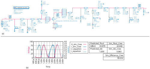
Figure 4 Initial physical Class E circuit design using a GaN device from Cree (a), which achieves good agreement between the predictions from the synthesis tool and the simulated waveforms on the device (b).
Figure 4 shows the actual first-pass physical circuit design created by following these four steps. For the input and output connections to the IC, EBOND components were used to model bond wires, and SMT components were used for blocking and bypassing. Otherwise, transmission lines were used for the matching.
The design produces similar waveforms, output power and DC current as compared with the idealized case, with 90 percent drain efficiency. These results track closely with the original prediction from the design synthesis utility used in Step 1. There is excellent agreement in both the waveforms and also the power and DC current. This accuracy is especially helpful for designers who are trying to maximize performance without losing reliability. To watch a short video describing this design, go to www.keysight.com/find/eesof-how-to-pa-series.
Conclusion
While designing a Class E PA can be difficult, a novel design process offers a simpler and faster alternative to the load-pull simulation technique. The process relies on first principles and allows designers to quickly get to a predictable and understandable starting point for the circuit. From here, designers can continue to make the models more accurate and physical and spend time on increasing bandwidth,4 ensuring stability over various conditions and minimizing the sensitivity of the circuit to process and packaging variation.

Matt Ozalas is a senior RF power amplifier and module design expert at Keysight Technologies, a position he has held since 2013. From 2001 to 2005, he worked at the Mitre Corp. doing RFIC and power amplifier design for a variety of high frequency applications. From 2005 to 2013, he worked at Skyworks Solutions in the Santa Rosa, Calif. Design Center, designing and developing high volume multiband power amplifier and front-end modules for wireless handsets. Ozalas received his BSEE from Penn State University in 2001 and his MSEE and MBA from Arizona State University in 2010.
References
- F. Raab, “Idealized Operation of the Class E Tuned Power Amplifier,” IEEE Transactions on Circuits and Systems, December 1977.
- A free copy of this workspace is available to download at www.keysight.com/find/eesof-how-to-pa-series.
- A. Grebennikov, N. Sokal and M. Franco, “Switchmode RF and Microwave Power Amplifiers, 2nd Edition,” Waltham, Mass., Academic Press, 2012.
- K. Chen and D. Peroulis, “Design of Highly Efficient Broadband Class-E Power Amplifier Using Synthesized Low-Pass Matching Networks, ” IEEE Transactions of Microwave Theory and Techniques, December 2011