
Microwave point-to-point links are an integral part of a cellular mobile network. Known as backhaul, they link cell sites (the BTS or Node B) and the radio controllers (the BSC or RNC) in over 50 percent of the global deployments, where fiber links are not cost effective. The market’s shift to smartphones has increased data traffic (e.g., streaming video), which is driving the capacity of microwave backhaul.
To scale the data throughput of the point-to-point radio network to meet the needs of LTE and LTE-Advanced, future generations of microwave links will need to
- Move to higher-order digital modulation, from today’s 256 QAM to as high as 4096 QAM. This will provide a 50 percent increase in capacity for a fixed channel bandwidth.
- Support channel bandwidths from 56 to 112 MHz in the traditional 6 to 42 GHz bands. Every doubling of channel bandwidth provides a proportional increase in the data throughput rate if the carrier-to-noise ratio (CNR) remains constant.
- Employ techniques such as polarization diversity, channel aggregation and n x n line-of-sight multiple-input-multiple-output (MIMO).
As is typically the case in communication system design, this increase in throughput capability comes at a price. Receiver sensitivity drops by 3 dB for every doubling in QAM or bandwidth, while the dynamic range of the link must increase to improve the error vector magnitude (EVM) performance.
Traditional backhaul systems split the radio into indoor (IDU) and outdoor (ODU) units. The RF/microwave section is in the ODU and connected with a coaxial cable to the rest of the system in the IDU. The cable, which can be up to 300 meters long, carries bidirectional traffic; a diplexer separates the receive (Rx) IF signal, centered at 140 MHz, from the transmit (Tx) IF, which is centered between 340 and 400 MHz.
The industry is moving to a single, self-contained outdoor unit (ODU), where the radio modem and transceiver are combined with the switching/multiplexing and traffic interface in a single box that is mounted on a tower or other structure. This trend is motivated by minimizing capital and operating expenses (CAPEX and OPEX) at new sites and limited space at existing sites. However, the legacy split IDU/ODU configuration will remain the majority of point-to-point shipments for the foreseeable future.
Modem Transceiver Designs
Given this evolving market, the back-end modem transceiver architecture should increase capacity and be compatible with both the legacy IDU/ODU and next generation ODU platforms. Additional design goals are to simplify the block diagram, relax the filtering and AGC requirements and reduce cost.
Recent advances in high speed digital-to-analog converters (DAC) and analog-to-digital converters (ADC) – operating at clock rates well above 1.5 GSPS – enable synthesizing and digitizing QAM signals at high IF frequencies with exceptional accuracy. DACs and ADCs now support 4096 QAM and eliminate the quadrature error correction that is usually required for analog IQ implementations. Their high dynamic range and oversampling ratio allow the majority of the filtering to be performed digitally, which reduces analog filtering and the digital equalization to compensate for it.
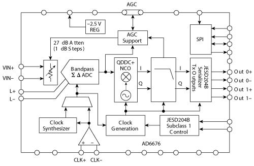
Figure 1 Block diagram of the AD6676 wideband IF receiver subsystem.
In the Tx path, high speed DACs are replacing the traditional dual DAC and IQ modulator implementations. They can synthesize the wideband QAM signals with exceptional EVM performance and do not require Tx calibration.
In the Rx path, most of the functionality of the IF receiver can be integrated into a single IC. The AD6676 is one such wideband IF subsystem; a block diagram of the IC is shown in Figure 1. Based on a bandpass sigma-delta (ΣΔ) ADC, it handles IF signal bandwidths up to 160 MHz, operating with an internal clock rate of up to 3.2 GHz. The high oversampling capability of the ΣΔ ADC greatly simplifies IF analog filtering requirements. ADCs operating at lower sampling rates require filtering to suppress adjacent channels and interference/blockers that would otherwise “alias” back onto the IF signal and reduce the receiver’s sensitivity.
The ADC in the AD6676 has a high dynamic range, with a noise spectral density (NSD) floor of -160 dBFS/Hz for narrowband QAM channels. This improves the analog AGC range, to compensate for fading, and reduces the required diplexer Tx-to-Rx isolation. The Rx subsystem includes a 27 dB digital attenuator with 1 dB resolution that can be used to calibrate the static gain error, caused by initial component tolerances and the variation in coaxial cable loss.
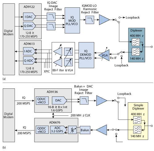
Figure 2 Comparison between legacy direct conversion IDU transceiver architecture (a) and architecture using high speed DAC and ADC for direct digital synthesis and digitization of the Tx and Rx QAM signals (b).
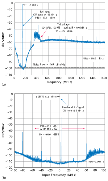
Figure 3 FFT of the AD6676 ADC output showing the spectrum of a CW signal with Tx leakage (a) and FFT of the IQ data following digital down-conversion (b).
The high speed DAC in the Rx IF subsystem both enhances performance and simplifies the IDU transceiver. Figure 2a shows the block diagram of a direct conversion transceiver with Rx and Tx IFs of 140 and 400 MHz, respectively. The challenges of direct conversion transceiver architectures are well documented. They can be overcome with IQ balance calibration, DC offset correction, tunable baseband IQ filtering and careful design of the diplexer to suppress Tx leakage. While transceivers with 256 QAM and channel bandwidths of 56 MHz are in production today, increasing the QAM constellation by 8´or more and doubling the channel bandwidth pose significant challenges to the direct conversion architecture. However the recent advances in high speed ADC and DAC technology enable a digital IDU architecture, as illustrated in Figure 2b. This transceiver requires only four ICs and delivers nearly perfect performance, with significantly relaxed filtering requirements.
A high speed DAC operating at a clock rate of 1.6 GSPS can synthesize a 112 MHz, 1024 QAM Tx signal with exceptional EVM performance. This allows the majority of the Tx link error budget to be reserved for the ODU, where the additive effects of phase noise and linearity degrade EVM the most. While a lowpass filter is required to suppress the first DAC image at 1.2 GHz, it can be relaxed up to 12 dB relative to the LO harmonic reject filter, which is needed to filter the IQ modulator’s third-order LO image that also falls at 1.2 GHz. Transmit power control to overcome cable losses can be performed within the IC, with negligible degradation of the EVM over a 15 dB range.
On the Rx side, the AD6676 digitizes the 112 MHz, 1024 QAM channel with excellent dynamic range and accuracy (see Figure 3), even with a large amount of Tx leakage from the “relaxed” diplexer filter. In this figure, the receiver subsystem was configured to support 112 MHz of channel bandwidth with its attenuator set to 3 dB, such that the effective noise figure referred to the input of the preamplifier was around 10 dB. The fast Fourier transform (FFT) response of the ΣΔ ADC data output (used only for the demonstration) is shown in Figure 3a. A CW tone of -17.2 dBm at 143 MHz represents the signal; the Tx leakage is centered at 400 MHz, with a power of -26 dBm.
The inherent “noise shaping” of the tunable bandpass ΣΔ ADC is evident in the region of high dynamic range centered about the desired IF, where the noise floor drops to -160 dBFS/Hz. Figure 3b plots the “zero IF” FFT response of the 16-bit, 200 MSPS IQ data after digital down-conversion and 16 x decimation filtering. The digital filter provides 85 dB rejection to remove the out-of-band noise and Tx leakage signal from aliasing back into the 112 MHz passband. The residual shaped noise falling outside the 112 MHz passband is removed by the modem’s root-raised-cosine (RRC) filters.
With this large CW signal of -2 dBFS, the in-band noise (IBN) was -68.6 dBFS. If a full-scale 1024 QAM Rx signal with a 10 dB peak-to-rms were to replace this CW tone, 7 dB of additional back-off would be required to prevent the ADC from clipping. In this case, the Rx IDU input power would be at -9 dBFS (-24.2 dBm), suggesting a CNR of nearly 60 dB.
To simplify the diplexer filter design, the diplexer Tx-to-Rx rejection would now be roughly 20 dB to suppress a -6 dBm Tx signal, such that the Tx leakage power would be -26 dBm at the input of the Rx preamp. For deployments with shorter cable runs between the IDU and ODU, the attenuator would be increased to tolerate higher QAM levels from the ODU.
The ability of the IDU receiver to recover a QAM signal at very low sensitivity levels in the presence of an unwanted signal nearby is an important specification (BER ≤ 10-6 with forward fault correction enabled). Perhaps the most demanding test (per ETSI EN 301 390 V1.2.1) is when a CW interferer tone (blocker) with 30 dB higher power than the QAM signal is only a 2.5x channel offset from the desired signal. Tunable or switched-bank filters employed in today’s receivers are mostly driven by this specification, since the modem must support channel bandwidths from 3.5 to 56 MHz. The previous example represents the next generation 112 MHz channel bandwidth case, where it is assumed that the adjacent CW interferer is sufficiently suppressed by a 112 MHz fixed channel filter that also performs image rejection, prior to the last down-conversion within the RF chain of the ODU. This same filter should provide sufficient blocker rejection at offsets of 70 and 140 MHz for the 28 and 56 MHz channel bandwidth cases. However, for channel bandwidths of 14 MHz or less, the CW tone will fall within this filter’s passband; this signal needs to be rejected with additional bandpass filtering at 140 MHz or digitized by the ADC and digitally filtered.
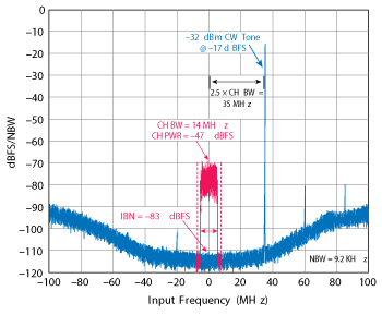
Figure 4 FFT of the IQ data showing the high dynamic range of the ADC provides design margin to tolerate adjacent interferers.
Advanced Architectures
An advanced ADC IDU receiver architecture has the instantaneous dynamic range to support this scenario without extra filtering. Figure 4 shows the FFT frequency response of the same Rx line-up used in Figure 3 except that the ΣΔ ADC’s tunable bandwidth was reduced to 56 MHz. In this example, a -32 dBm CW tone at 175 MHz (or 35 MHz offset) was added to the ever present -26 dBm Tx leakage signal at 400 MHz. This CW tone corresponds to a -17 dBFS input level seen by the ADC and is set to be 30 dB higher than a -47 dBFS 1024 QAM signal at minimum sensitivity (CNR = 36 dB). The CW interferer can be increased by an additional 15 dB, highlighting the design margin that can be allocated to the microwave circuitry’s noise contribution. In the absence of the blocker, the desired 1024 QAM signal level can be increased by 38 dB, offering additional dynamic range for the IDU receiver to compensate for fading.
The same dynamic range benefits that an advanced ADC offers for the IDU design can be used in a self-contained ODU receiver design. Figure 5 shows the receiver block diagram for an 18 to 23 GHz ODU with dual down-conversion prior to the IF receiver. Other microwave bands in the 6 to 43 GHz range can be supported with the same IF receiver subsystem by selecting the appropriate image reject mixers, phase-locked loops and, possibly, changing the first IF frequency.
With a single ODU, where there is no cable to limit the IF choices, the ADC can be set to a higher IF, such as 300 MHz, which further simplifies the RF image-rejection filtering. The ADC can connect directly to the RF mixer or, should any of the larger mixer spurs require additional suppression, via a simple third-order lowpass roofing filter. The RF filter at 1960 MHz handles channel bandwidths up to 112 MHz. With the ADC attenuator at 0 dB, the combined noise floor is below -157 dBFS/Hz for channel bandwidths of 56 MHz, which is an equivalent NF of 17 dB. The default total conversion gain can be initially optimized with the instantaneous dynamic range, such that the digital modem tracks initial fading from nominal Rx input power levels. The AGC threshold can be set to increase the gain when the modem’s Rx BER drops below a predetermined level for a specified QAM signal level. This hybrid approach only activates the RF AGC if the input levels are very low, to improve the receiver’s minimum sensitivity level.
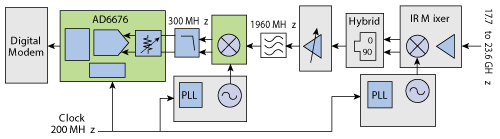
Figure 5 Block diagram of dual down-conversion ODU radio using the wideband IF receiver subsystem.
Conclusion
To increase data rates, next generation microwave point-to-point radios will utilize higher QAM modulation and channel bandwidths up to 112 MHz, and they must have the dynamic range to maintain BER performance with signal fading. Advances in ADC and DAC technology are enabling modem transceivers to support these changes, while also simplifying the architecture. For split IDU/ODU systems, wideband IF receivers such as the AD6676 offer exceptionally high dynamic range to ensure excellent modulation accuracy (EVM) in the presence of adjacent interfering signals, without needing complicated tunable or bulky switched-bank filters. For single ODU systems where the receiver can directly interface with the down-converting mixer, the high instantaneous dynamic range of the receiver reduces RF filtering requirements and the RF AGC range to compensate for fading.