
Radical industry structural change is imminent due to the convergence of an unprecedented demand for bandwidth and the continuing advancements being made in the silicon industry. At the center of this shift, modern military systems and next generation communication devices will feature active electronically steered antennas (AESA) and operate at mm-wave frequencies using highly integrated silicon core chips. When these core chips are coupled with advanced system architectures, a disruptive and refreshing change to our industry will result.
Multiple trends are simultaneously occurring in the industry today: 1) AESAs in the aerospace and defense (A&D) industry are increasingly being required to be “multi-function,” i.e. capable of supporting both communication and radar applications from the same array; 2) both A&D and commercial AESAs are moving toward increasingly complex system architectures that feature silicon core chips supporting multiple radiating elements, multiple independently steerable beams, polarization flexibility, and interfacing with smaller amounts of III-V material at each radiating element; 3) AESAs are evolving toward low profile implementations where all electronics reside within the lattice constraints of the array thus forcing higher levels of integration within the silicon core chips; 4) systems are focusing on size, weight, power, and now cost (SWAP-C) where incumbent GaAs-based designs are being displaced by more cost effective silicon solutions; and 5) the demand for bandwidth in next generation communications systems is forcing a migration to mm-wave frequencies and AESAs with steerable beams that offer frequency re-use through spatial diversity. These trends are forcing a powerful disruptive change to the global communications and radar industries.
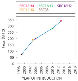
Figure 1 Evolution of SiGe HBT devices (courtesy of TowerJazz).
Demand for Bandwidth Driving Spectrum Expansion and AESAs
The demand for bandwidth is predicted to increase 1000× from 2010 to 2020 with mobile connected devices over the same period increasing from 5 to 50 billon devices.1 This demand is unprecedented in the industry and is fueling the need for increased spectrum allocations for next generation systems. Traditional cellular and RF bands below 6 GHz are not equipped to meet the demand with global allocations being non-contiguous in nature and aggregating to only 780 MHz.2 This is pushing the interest to mm-wave frequencies with current 5G activities on-going at 28, 39, 60 and E-Band frequencies where large contiguous bands of spectrum are available. Increased spectrum and the spatial reuse of AESA steerable beams are a compelling solution to meet these high bandwidth demands.
New 5G architectures envision AESAs imbedded in mobile devices to connect with existing 3G/4G base stations via narrow steerable beams over short ranges (<200 m). Mm-wave arrays can offer high directivity in small footprints which offsets the higher path loss associated with mm-wave operation.3 The antennas will search out best line of sight or reflected signals for system connectivity.4 Due to the high number of expected mobile devices requiring this technology, the cost structures of such arrays must be very low which is where silicon becomes critical.
Silicon Enabling AESA Advancements
Advances in silicon have followed Moore’s Law since the 1960s, which has resulted in silicon devices that now can operate quite successfully at millimeter wave frequencies.5 For example, Figure 1 illustrates the continuous improvements in silicon germanium HBT devices since the year 2000 with present devices achieving Fmax in excess of 300 GHz. This enables feature rich solutions for next generation mm-wave AESAs that will displace traditional, more expensive GaAs solutions. The ability to integrate RF, analog and digital hardware onto a single die provides a compelling reason to go to all silicon solutions for low cost AESAs. Add to this the fact that silicon based phase steering circuits are lumped element in nature rather than distributed, which allows silicon solutions to operate over wider frequency bands and be realized in very compact die sizes.
The latest phased array antenna solutions are evolving into silicon core chips that support multiple radiating elements, or for applications that require the best possible performance, silicon core chips plus III-V front ends such as GaAs or GaN. The III-V front ends are used to establish best possible NF and output power. Another significant trend occurring in the industry is that GaN is displacing GaAs as the material of choice for high power or broadband front ends. As the cost of GaN continues to decrease, the eventual elimination of GaAs from phased antennas could be expected for many applications.
Historical Review of Silicon-based Core Chips
AESAs have historically been GaAs-based solutions confined to the aerospace and defense markets, but modern silicon based AESAs are now penetrating a multitude of military and commercial markets. These silicon RFICs are now seen as a technology which has allowed a drastic reduction in phased-array cost up to 110 GHz.
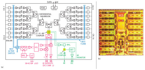
Figure 2 16-element 77 to 84 GHz phased array with integrated Rx and BIST layout (a) and chip (b). (Reprinted with permission from UCSD).
These SiGe chips which contain amplitude and phase control and the required digital interface and control, were first developed as single-elements by Raytheon, Boeing and Professor Rebeiz’s group6-8 but enjoyed a huge leap in performance and integration density with the demonstration of the first RF-beamforming SiGe 6 to 18 GHz, 8-element phased-array receiver chip with 5-bit phase control and an on-chip 8:1 combiner.9 Shortly thereafter, the first 16-element 45 to 50 GHz phased array transmitter was demonstrated.10 More recently, accurate on-chip built-in-self-test (BIST) at W-Band has been demonstrated, and showed that such techniques can drastically reduce the testing and calibration time (see Figure 2).11,12
Demonstrating even higher levels of integration was the first wafer-scale phased array at 110 GHz where high efficiency antennas are directly integrated on-wafer and a full phased-array is achieved without any dicing or mm-wave packaging.13

Figure 3 16-element W-Band Tx+2Rx polarimetric radar RFIC. (Reprinted with permission from UCSD).
The effect of silicon core chips on the industry has been phenomenal. First, the UCSD work has triggered a large set of defense programs including the ONR Integrated Topside program for advanced AESAs. The 8- and 16-element AESAs with RF-beamforming have become the basis of several 60 GHz communication systems by IBM, Intel, SiBeam and others.14-16 Toyota, together with UCSD, developed a 77 GHz FMCW radar based on a 16-element phased-array receiver and capable of achieving pedestrian detection at large distances and in high-clutter environments.12,17,18 The silicon AESAs are also used in a large number of SATCOM systems from X- through Q-Band, both with single and multiple beam capabilities. Recently, SiGe phased array chips with 16-elements and fully polarimetric transmit/receive capabilities have been demonstrated at W-Band frequencies for helicopter landing systems (see Figure 3).19 It is no exaggeration to state that every commercial or defense phased-array program developed to-date includes a large SiGe (or CMOS) component, and this is resulting in much more complex and lower-cost phased array than previously imagined.
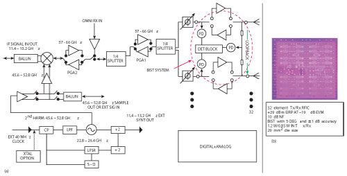
Figure 4 32-element 60 GHz Tx/Rx RFIC with BIST layout (a) and chip (b)20.

Figure 5 Half-wavelength area available for parts as a function of operating bands.
mm-wave AESA Example
Intel’s Mobile Wireless Group in Haifa, Israel published results for a 32-element 60 GHz transmit/receive AESA implemented on 90 nm CMOS.20 The chip is shown in Figure 4 and is intended to enable wireless docking in laptop computers. The AESA features a single steerable beam, 32-way analog beamforming, 4-bit phase control, and up/down conversion to/from 12 GHz. When combined with radiating elements implemented in a low cost LCP package, the chip demonstrated >5 GBPS data rate using 16-QAM modulation. The die is 29 mm2 and consumes 1.2 W of DC power. This achievement demonstrates the ability of silicon to provide excellent performance and cost points at mm-wave frequencies.
Lattice Considerations for Planar AESAs
In any AESA, as the frequency of operation increases, available surface area for parts decreases. Figure 5 shows the relative surface area for a half-wavelength by half-wavelength “unit cell” for phased arrays at X- through Q-Band superimposed with packaged GaAs parts that constitute a single beam steering channel. This decrease in available surface area eliminates this GaAs architecture from being a useful technology for single beam planar AESAs above Ku-Band. For AESA applications that require more than a single beam, planar applications above X-Band require a silicon solution.
SiGe and RF CMOS enable significantly higher integration of RF functions into a single RFIC, allowing higher frequency planar arrays. Figure 6 shows the relative area of 16 GaAs MMIC phase shifters compared to one 16 Channel SiGe RFIC at Ku-Band. The sixteen GaAs die, each approximately 2.2 × 2.2 mm, take up a total die area of about 77 mm2 for the phase shift function alone, compared to the SiGe RFIC, with a total area of about 25 mm2. The additional benefits of the SiGe MMIC are inclusion of RF amplifiers, RF combining and dividing networks, digital control logic, calibration tables, temperature sensing and compensation, and voltage regulation. Thus a 25 mm2 die with 16 independent channels (i.e., one phase shifter per channel) could support a 4 × 4 sub-array, enabling planar arrays operating above 100 GHz.

Figure 6 Relative area of 16 GaAs phase shifter die compared to the area of one 16-channel SiGe phased array die.
Importance of Systems Engineering
Systems engineering plays a key role in the convergence of silicon and mm-wave frequencies. As the industry shifts toward highly integrated, feature rich core chips, it is increasingly important that RFIC developers have in-house systems engineering expertise to help their customers reap all the benefits that the complex technologies have to offer. The systems engineer can assist the customer in selecting the optimum monolithic process(es) for the application at hand. For example, is an all silicon approach the most appropriate or will some III-V MMICs be warranted? What about an interface control chip between the low voltage silicon core chip and the higher voltage III-V chips? Having the RFIC systems engineer assist with early architecture definition enables the customer to optimize their system and allows them to extract maximum value from it.
Companies like Anokiwave operate with this systems engineering design setup and have designed 20/30 GHz SATCOM and 24 GHz automotive radar solutions.21,22 Figure 7 shows a highly integrated FMCW radar transceiver implemented in 180 nm BiCMOS SiGe technology with this approach.
Future Considerations for Our Industry
Since the industry is rapidly evolving, it is important to look forward and assess what the systems of the future will look like. Motivation to get from antenna-to-bits will become increasingly important and will involve pulling digital capability as close to the radiating element as possible. Replacement of RF front end components with high speed digital signal processing components will become the norm. The steady advance of Moore’s Law will generate continually higher speed devices allowing mm-wave and high speed digital circuits to coincide on the same RFICs. Within the next decade we can also expect to see a multitude of everyday devices like garage door openers, videos players, computers, etc. all communicating with each other wirelessly levying ever higher demands on bandwidth. Massive MIMO at mm-wave will be commonplace and will require highly compact, ultra-low cost multi-beam AESAs to be imbedded in everyday devices. It is clear that the industry will continue to advance at a dizzying pace and require ever higher levels of functional integration at consumer cost points.
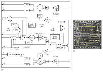
Figure 7 Highly integrated 24 GHz FMCW SiGe BiCMOS transceiver layout (a) and chip (b) (reprinted with permission from ViaSat Inc.).
Conclusion
The industry is at a juxtaposition where the exponential demand for increased data rates coupled with Moore’s Law’s relentless march are enabling low cost mm-wave AESA solutions, new radars, communication systems and even 5G handsets in the near future. The industry is indeed at a tipping point.
References
- http://spectrum.ieee.org/telecom/wireless/, “Millimeter Waves May Be the Future of 5G Phones,” Ariel Bleicher, June 13, 2013.
- http://ieeexplore.ieee.org/xpl/articleDetails.jsp?reload=true&arnumber=6515173, “Millimeter Wave Mobile Communications for 5G Cellular: It Will Work!,” T.S. Rappaport, et al., NYU WIRELESS,February 3, 2013.
- “Coverage and Capacity Analysis of mmWave Cellular Systems,” Robert W. Heath, Jr, University of Texas, June 15, 2013.
- http://nsn.com/news-events/insight-newsletter/articles/, “5G Ultra-Wideband Enhanced Local Area Systems at Millimeter Wave,” September 3, 2013.
- “State of the Art in 60-GHz Integrated Circuits and Systems for Wireless Communications,” T.S. Rappaport, et al., Proceedings of the IEEE, August 2011.
- R. Tayrani, M.A. Teshiba, G.M. Sakamoto, Q. Chaudhry, R. Alidio, Y. Kang, I.S. Ahmad, T.C. Cisco and M. Hauhe, “Broad-Band SiGe MMICs for Phased-Array Radar Applications,” IEEE Journal of Solid-State Circuits, Vol. 38, No. 9, September 2003, pp. 1462-1470.
- T.M. Hancock and G.M. Rebeiz, “A 12 GHz SiGe Phase Shifter with Integrated LNA,” IEEE Transactions on Microwave Theory Technology, Vol. 53, No. 3, March 2005, pp. 977-983.
- B.W. Min and G.M. Rebeiz, “Ka-Band BiCMOS 4-Bit Phase Shifter with Integrated LNA for Phased Array T/R Modules,” IEEE International Microwave Symposium, Honolulu, HI, June 3-8, 2007, pp. 479-482.
- K. Koh and G.M. Rebeiz, “An X- and Ku-Band 8-Element Phased-Array Receiver in 0.18-µm SiGe BiCMOS Technology,” IEEE Journal of Solid State Circuits, Vol. 43, No. 6, June 2008, pp. 1360-1371.
- K. Koh and G.M. Rebeiz, “A Millimeter-Wave (40-45 GHz) 16-Element Phased-Array Transmitter in 0.18-µm SiGe BiCMOS Technology,” IEEE Journal of Solid State Circuits, Vol. 44, No. 5, May 2009, pp. 1498-1509.
- O. Inac, D. Shin and G.M. Rebeiz, “A Phased Array Chip with Built-In Self-Test Capabilities,” IEEE Transactions on Microwave Theory and Techniques, Vol. 60, No. 1, January 2012, pp. 139-148.
- S.Y. Kim, O. Inac, C.Y. Kim, D. Shin and G.M. Rebeiz, “A 76-84 GHz 16-Element Phased Array Receiver with a Chip-Level Built-In Self-Test System,” IEEE Transactions on Microwave Theory and Techniques, Vol. 61, No. 8, August 2013, pp. 3083-3098.
- W. Shin, B. Ku, O. Inac, Y.C. Ou, and G.M. Rebeiz, “A 108-116 GHz 4x4 Wafer-Scale Phased Array Transmitter with High-Efficiency On-Chip Antennas,” IEEE Journal Solid-State Circuits, Vol. 48, No. 9, September 2013, pp. 2041-2055.
- A. Valdes-Garcia, S.T. Nicolson, J. Lai, A. Natarajan, P. Chen, S.K. Reynolds, J.C. Zhan, D. Kam, D. Liu and B. Floyd, “A Fully Integrated 16-element Phased-array Transmitter in SiGe BiCMOS for 60 GHz Communications,” IEEE Journal of Solid-State Circuits, Vol. 45, No.12, December 2010, pp. 2757–2773.
- E. Cohen, C. Jakobson, S. Ravid and D. Ritter, “A Thirty Two Element Phased-array Transceiver at 60 GHz with RF-IF Conversion Block in 90 nm Flip-chip CMOS Process,” IEEE Radio Frequency Integrated Circuits Symposium, May 2010, pp. 457-460.
- S. Emami, R.F. Wiser, E. Ali, M.G. Forbes, M.Q. Gordon, X. Guan, S. Lo, P.T. McElwee, J. Parker, J.R. Tani, J.M. Gilbert and C.H. Doan, “A 60 GHz CMOS Phased-array Transceiver Pair for Multi-Gb/s Wireless Communications,” IEEE International Solid-State Circuits Conference, San Francisco, CA, USA, February 2011, pp. 164-166.
- B. Ku, P. Schmalenberg, S. Kim, C. Kim, O. Inac, J. Lee, K. Shiozaki and G.M. Rebeiz, “A 16-Element 77–81-GHz Phased Array for Automotive Radars with ±50° Beam-Scanning Capabilities,” IEEE International Microwave Symposium, June 2013, pp. 1-4.
- B.H. Ku, O. Inac, M. Chang and G.M. Rebeiz, “A 75-85 GHz Flip-Chip Phased Array RFIC with Simultaneous 8-Transmit and 8-Receive Paths for Automotive Radar Applications,” IEEE Radio Frequency Integrated Circuits Conference (RFIC), June 2013, pp. 1-4.
- F. Golcuk, T. Kanar and G.M. Rebeiz, “A 90-100 GHz 4×4 SiGe BiCMOS Polarimetric Transmit-Receive Phased Array with Simultaneous Receive-Beams Capabilities,” IEEE Transactions on Microwave Theory and Techniques, Vol. 61, No. 8, August 2013, pp. 3099-3114.
- E. Cohen et al., “A CMOS Bidirectional 32-element Phased-array Transceiver at 60 GHz with LTCC Antenna,” Radio Frequency Integrated Circuits Symposium (RFIC), June 2012, pp. 439-442.
- S. Lorg et al., “Single Chip K-band Transceiver ASIC with Internal PLLs, Image Reject Mixer, and Multiplexed IF,” GOMAC Tech 2011, section 8.4.
- Dave Saunders et al., “A Single-Chip 24 GHz SiGe BiCMOS Transceiver for Low Cost FMCW Airborne Radars,” Aerospace & Electronics Conference (NAECON), Proceedings of the IEEE 2009 National, July 2009, pp. 244-247.