
Editor’s Note: We are at an exciting time in our industry where several technologies seem poised to start replacing incumbent technologies that have performed well for many years causing a large shift in the marketplace. These new technologies provide the same or better performance at a significantly lower cost and smaller footprint.

CMOS PAs have traditionally not been able to match the performance of GaAs PAs but now have accomplished that in the form of handset front end PA modules even in 4G/LTE applications. With a much lower cost structure and higher level of integration, CMOS is now positioned to penetrate the high volume handset front end market.
GaN has been able to outperform GaAs PAs and challenge LDMOS PAs but because it has been more expensive it has had only limited success in some high performance markets. This is changing as GaN on Si is ready to scale to 8 inch wafers and use low cost plastic packaging techniques that will significantly reduce the cost of GaN on Si and allow it to become a mainstream solution in the RF industry. Microwave Journal solicited the following two pieces from companies well positioned to challenge the status quo with CMOS and GaN technologies.
Reconfigurable CMOS RF Front End
Duncan Pilgrim
Peregrine Semiconductor, San Diego, CA
CMOS technology rapidly dominates any market where it meets the required performance. The reason is clear – the incredible amount of investment in CMOS technology has led to massive manufacturing scale and continuous process technology improvements. When CMOS reaches the equivalent performance, it represents an inflection point for rapid transition from an incumbent technology to CMOS. This principle is well understood in the RF industry – advancements in CMOS always yield a disruption in the marketplace.
Changing the Status Quo in the RFFE
In 2004, Peregrine Semiconductor introduced its first CMOS-based cellular antenna switch, which earned market share in size-critical products due to the high level of integration and the small footprint. However, it did not meet all of the RF performance metrics, primarily insertion loss of the incumbent GaAs switches. But the release of UltraCMOS® 5 technology offered the market all of the benefits of integration, size and quality and also superior performance to GaAs switches. A key figure of merit used to compare the performance of switch devices is RONCOFF. In a perfect switch the RON would be zero, resulting in zero insertion loss, and the COFF would be zero, resulting in infinite bandwidth. With UltraCMOS 5 technology, the RONCOFF was 253 fs, which was for the first time below that of GaAs processes. The impact of this combination of high-level CMOS integration with GaAs-level performance can be best illustrated by the resulting volume of shipped products. It took 10 years to ship the first billion chips into the market; following the UltraCMOS 5 technology introduction, it took less than two years to ship the 2nd billion. Currently, GaAs antenna switch suppliers are transitioning to CMOS to remain competitive in the market. With the introduction of the UltraCMOS 10 technology in 2013 and the UltraCMOS Global 1 RF front end (RFFE) in 2014, another performance milestone in CMOS performance has been achieved, this time with the potential to allow CMOS-based power amplifiers (PA) to overtake GaAs-based power amplifiers–even in the high-end LTE smartphone market.
The Next Inflection Point
The UltraCMOS Global 1 system introduces the first reconfigurable RFFE, accommodating all 40-and-growing LTE bands, which allows OEMs to develop a single-SKU product for all global mobile device markets and provides engineers with tunability to simplify the design and testing of more than 5,000 times increase in possible RFFE states. The reconfigurable RFFE is based on an RF silicon on insulator (SOI) CMOS technology that has a foundation of more than 170 filed and pending patents along with proven manufacturing capability that has resulted in more than 2 billion units shipped.
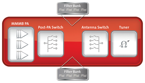
Figure 1 Peregrine's UltraCMOS® Global 1 is the first reconfigurable RFFE system.
Architecture Overview
This integrated RFFE solution based on the UltraCMOS 10 technology platform offers an architecture that is 100 percent CMOS-based, which enables all components to be integrated including (see Figure 1):
- 3-path, multimode, multiband PA
- Post-PA switch
- Antenna switch
- Antenna tuner
- Common RFFE MIPI interface
A key factor in Global 1’s design is the UltraCMOS 10 technology platform, a 130 nm RF SOI technology manufactured in partnership with GLOBALFOUNDRIES. This recent process delivers a 50 percent performance improvement as measured using the RONCOFF figure of merit over comparable RF SOI processes.
Each component supports the demanding linearity, isolation and low loss requirements for LTE devices and is tightly integrated in the system. This combination of performance and integration simplifies the design process and reduces the total RFFE footprint as much as 50 percent. All of the functions are controlled through a common MIPI RFFE 1.0 interface, allowing easy integration onto platform vendors’ reference designs.
Supporting Technologies
The RFFE meets – and, in certain bands, exceeds – the raw power added efficiency (PAE) of current alternatives, that are based on a hybrid of SOI, bulk CMOS and GaAs technologies. When supporting technologies, such as envelope tracking and digital pre-distortion (DPD), are added, they further enhance the technology’s performance advantage. Global 1 is designed to seamlessly integrate onto any reference-design platform and can use any third-party filters and envelope-tracking modulator, allowing the flexibility to select the components that optimize performance and/or cost based on the unique criteria of the reference design.
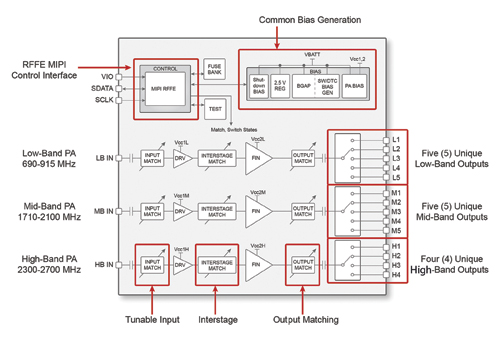
Figure 2 Peregrine's UltraCMOS Global 1 PA can exceed the performance of GaAs-based LTE PAs and offers substantially more integration benefits.
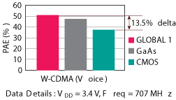
Figure 3 The Global 1 PA has better performance than GaAs and exceeds the performance of existing CMOS PAs by 13.5 percentage points.
Power Amplifier
Before now, GaAs was the only technology capable of delivering power amplifiers with the high performance LTE devices require. After eight years of research and development, this technology represents one of the first CMOS SOI power amplifiers to meet the performance of GaAs-based products. The
UltraCMOS Global 1 PA (see Figure 2) is a multimode, multiband PA that monolithically integrates the three amplifier paths – bias generation and control – via a MIPI interface.
The post-PA switches are integrated onto the same die as the PA, so it can support five unique bands for low band, five unique bands for mid band and four unique bands for high band. The PA supports a range of frequencies: 690 to 915 MHz in the low band, 1710 to 2100 MHz in the mid band and 2300 to 2700 MHz in the high band. In recent years a single, high-band path was all that was required, and this was cost-effectively supported via the use of a satellite PA. Today’s devices must support as many as four different high-frequency bands, and the integration of the high band is critical in order to support the roll out of bands – 38 and 40 for the TD-LTE network in China, B7 in Europe and Hong Kong, B41 in the United States and other bands in various geographic locations.
PA Performance
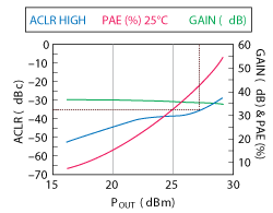
Figure 4 This real-time performance test shows a drive-up curve in which the red line indicates the PAE and the blue line indicates the ACLR.
A standard industry benchmark for PA performance is PAE using a W-CDMA (voice) waveform at an adjacent channel leakage ratio (ACLR) of -38 dBc. Under these conditions, the performance of the low band, multimode, single-band (MMSB) PA is more than 50 percent PAE (see Figure 3). This surpasses the leading GaAs PAs and exceeds the performance of other CMOS PAs by 13.5 percentage points. Initial Global 1 figures released in February displayed the Global 1 PA matching the performance of GaAs PAs and exceeding CMOS PAs by at least 10 percentage points. However, after continued product development, Peregrine is reporting a higher level of performance – a level that exceeds GaAs PAs in certain bands.
The PA is not limited to W-CDMA – using e-UTRA test conditions, Figure 4 shows a typical LTE drive-up curve with a 25 resource block (RB) QPSK signal at 782 MHz. The ACLR1 is very well behaved, and the PA has been designed to work over the entire output power range. At -35 dB ACLR, the PA achieves approximately 43 percent efficiency for a MMSB PA using a 25 resource block (RB) QPSK signal at 782 MHz. These curves are very similar to the performance of a state-of-the-art GaAs PA.
The data in Figure 5 shows that GaAs-equivalent performance is maintained for LTE waveforms (RB) allocations up to 100 RB. The level of performance achieved is in line with current high-end GaAs PAs. Similar competitive results have been achieved in mid and high bands of operation. The CW measurements show performance when the PA runs into saturation and is a good indication of the approximate performance that can be achieved when envelope tracking is added.
Adding Envelope Tracking
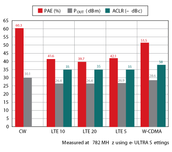
Figure 5 Across the low band, the UltraCMOS Global 1 PA shows little performance roll-off with W-CDMA, LTE5, LTE10 and LTE20 waveforms.
Achieving the efficiency benefits of envelope tracking while still meeting linearity and noise requirements has proven challenging. Now a number of envelope-tracking modulators meet all of the requirements. Most modulators have unique architectures that impose slightly different requirements on the PA, but certain commonalities in the requirements exist, including minimizing the AM-AM / AM-PM distortion characteristics of the PA and maintaining a consistent gain response down to low-drain voltages. Careful design of the biasing structures and PA architecture are critical in achieving these requirements. Integrating the bias circuits and the PA together enables tight control across process, voltage and temperature (PVT) and reduces the variation of these effects.
As with traditional GaAs-based PAs, the UltraCMOS Global 1 PA gains performance improvement with envelope tracking (ET). Peregrine’s PA configurability enables the match and the biasing to be optimized based on the selected ET solution. As such, the design can support a broad range of ET modulators, giving engineers a full range of choice for optimizing their reference designs.
As an example, Peregrine has completed testing using Nujira’s NCT-L1300 envelope tracker in conjunction with an UltraCMOS MMSB PA. This combination yields a more than an 18 percent point PAE performance improvement (see Figure 6) and results in a system efficiency of more than 50 percent. The data is taken at 780 MHz using a 25 RB QPSK LTE signal with a PAPR of 7.3 dB. The results are measured at a 29.8 dBm with an ACLR -38 dBc. These results are taken using a linear output match and modulating only the final-stage supply. It is possible to gain more performance improvement if the supply of the driver is also modulated and if the match is optimized for saturated operation.
PA Configurability
The combination of tunable matching and extensive bias control allows the device to be configured based on the mode, power and frequency of operation. Configurability has become a necessity in the RFFE as the number of frequency bands and modes that devices need to support grows. China Mobile, for example, is targeting phones that support ten bands and five modes, and this trend is expected to continue. With all of these modes, band combinations, power levels and other factors, the number of possible states grows exponentially. Peregrine estimates that there will be more than a 5,000 fold increase in the number of possible states of the RFFE. Consider that there are more than 150 different switch elements integrated on the Global 1 die, and all of these must be controlled and routed. This level of control and configurability can only be economically implemented with a fine-geometry CMOS process.
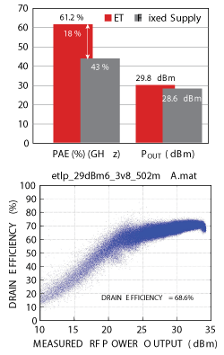
Figure 6 When Nujira's envelope tracking is added, the Global 1 PA's PAE performance increases by 18 percentage points; output power increases by more than 4%; and the drain efficiency exceeds 68%.
Support for Multiple Frequency Bands
Global 1’s CMOS-based process enables monolithic integration of low-loss switches, digitally tunable capacitors, high-Q on-chip passives and control circuitry, and it includes tunable matching networks enabling load-line optimization. This results in an RFFE that is frequency agile and can be tuned and optimized for the band of operation.
Each path of the power amplifier covers a wide frequency range, and, within this range, there are multiple 3GPP frequency bands – 11 are in the low band alone. Currently, engineers have two choices for supporting multiple frequency bands in a single device. One option is to have a PA and a duplexer per supported band, which offers the highest performance but can be expensive and prohibitive due to the amount of real estate this consumes. The second option is to use a multimode, multiband (MMMB) PA, which is capable of supporting broadband operation; in low band this would require support from 699 to 915 MHz. With the MMMB PA option, engineers must accept lower performance across the entire band. GaAs PAs minimize output-power degradation across the band well, but the PAE curves show significant roll-off. For example, the PAE could be very high at 900 MHz but could drop by as much as 10 to 12 percent at 700 MHz. With Peregrine’s fully tunable PA, engineers can optimize ACLR, output power and PAE for each desired band of operation.
Interfacing Into the Duplexers
In a traditional MMMB PA – where the output match (ZO) is fixed – it is not possible to provide an optimal match into all of the different duplexers as shown in Figure 7. The match can either be optimized for one of the paths which results in degraded performance for all other paths, or the match can compromise performance in all bands but to a lesser extent.
Mismatches between PAs and duplexers can lead to increases in insertion loss of tenths of dB’s equating to percentage points of reduction in PAE. This has been a major factor in the success of the single-band PA with integrated duplexer (PAiD) modules, which have been used extensively by OEMs that are focused on the highest performance possible.
The alternative is a MMMB PA that includes a tunable output match (see Figure 8) that can be tuned based on the band of operation. This PA offers band specific optimization of the interface impedance that has traditionally only been possible with PAiD modules.
With impedance tuning, ZOX is effectively re-tuned so that the output of the MMMB PA is matched to the input impedance of the duplexer on a per-band basis.
Z013 = ZIN13; Z017 = ZIN17; Z05 = ZIN5; Z08 = ZIN8 & Z025 = ZIN25
This tunability enables the device to easily work with any filter products on the market, and it reduces the benefit of co-packaging the filter elements with the rest of the solution. In addition, Global 1 supports external filters and can be easily configured to support different frequency bands and combinations.
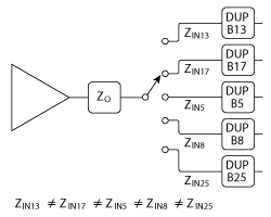
Figure 7 In this block diagram of a traditional MMMB PA and duplexer, there is no way to provide an optimal match from the PA to all duplexers.
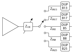
Figure 8 Global 1 integrates a tunable output match, enabling optimized performance for all paths.
Configurability
The tunable PA helps engineers achieve multiband operation with minimal performance degradation and a host of additional benefits, including:
- Removal of production make tolerances
- Temperature compensation to minimize variation across the temperature range
- Optimization for the different modes and power levels
- Match re-tuning for envelope tracking or for average power tracking
- Compensation for mismatches between the PA and duplexer, antenna or even variations in PCB layout
RF design engineers will benefit most from the UltraCMOS Global 1 system because it can dramatically reduce the engineering and validation time required. Platform providers can develop a single reference platform, reducing reference design development costs and validation time. The ability to electronically tune the frequencies of operation means that the traditional hand tuning required to get the “optimal” performance can now be completed by running an optimization program overnight. OEMs can quickly optimize the reference design based on the feature set and form factor of the product. This cuts research and development costs, accelerates time to market, streamlines supply chains and improves inventory management. Consumers can enjoy longer battery life, better reception, faster data rates and a wider roaming range.
Conclusion
Why now? Just look at what is going on in the LTE market as noted in the ABI Research report “The Connected World of Tomorrow: Predictions for 2014 and 2015.” According to that report, there are 375.2 million LTE subscriptions in 2014, and that number will increase by more than 60 percent, to 588.9 million, in 2015. In addition, 4G-mobile-network data traffic will more than double in 2014, reaching 12.4 exabytes. These demands require an unprecedented RFFE performance. What is needed is a true disruption in the marketplace.
History has shown that true innovation and forward progress is the result of challenging the normal way. To meet this challenge, Peregrine has developed a fully reconfigurable RFFE designed on an advanced CMOS platform based on 25 years of RF expertise. The final piece of the complete system – introduced in February 2014 – is an LTE-class, CMOS PA that exceeds the performance levels of GaAs-based alternatives, delivering reconfigurability and performance that make possible a single, global SKU accommodating all 40+ LTE bands and more than 5,000 RF states. The resulting system provides greater flexibility and choice to help RF engineers meet the next wave of global, mobile-device innovation.
Mainstream Commercialization of GaN
Doug Carlson
MACOM, Lowell, MA
The performance advantages that are achievable with GaN technology are well known to all involved with the RF and microwave industry today. GaN delivers as much as eight times the raw power density of incumbent GaAs and LDMOS technologies at high efficiency, with the ability to scale the device technology to high frequency. GaN technology has allowed device designers to achieve broad bandwidths while maintaining high efficiency. It has also shown to perform well in high power switching and LNA applications.
GaN technology development has been driven primarily by government funding and R&D. GaN on Silicon Carbide (SiC) is being successfully applied in the military domain today for applications including broadband electronic warfare jammers and radar systems, while GaN on Silicon (Si) has been successfully deployed in military communications. This activity has opened the door for GaN’s penetration into commercial markets including CATV, cellular infrastructure and other applications, and we are seeing the initial penetration of GaN into these markets now.
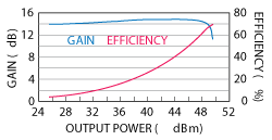
Figure 9 GaN on Si performance example, 100 W device at 2.7 GHz, 48 V Vds.
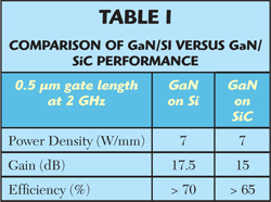
In order to accommodate the unique price/performance requirements of these diverse commercial applications, GaN will remain segmented into two distinct varieties: GaN on SiC for specialized high performance applications, and GaN on Si for cost-sensitive volume applications. MACOM is positioned to evaluate these two varieties of GaN as they market a broad portfolio of pulsed and CW products based on both SiC and Si substrates. At the device level, the performance of GaN/Si and GaN/SiC are essentially identical (see Table 1).
GaN technology is reaching its potential – solving both the technical and cost challenges is critical to its mainstream commercial adoption. On the technical front, MACOM has recently demonstrated device performance, targeting significant commercial applications (see Figure 9 as an example), that demonstrate that GaN on Si is a leading candidate as the next generation RF power technology to counter today’s incumbent silicon based solutions. GaN on Si has achieved the output power, efficiency, gain, bandwidth and operating voltages that, when coupled with a silicon based manufacturing roadmap and associated cost structure, demonstrate why GaN is revolutionizing the RF industry.
In addition to offering compelling performance, GaN on Si has proven device reliability. At both 28 and 48 V bias, MACOM’s GaN on Si HEMT processes demonstrate excellent reliability as demonstrated with three temperature accelerated life testing. The life test results, using a 20 percent change in IDSS as the criteria of failure, result in an MTTF of 1x10⁶ hours at 200°C junction temperature with an activation energy of 2.2 eV (see Figure 10).
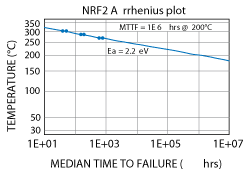
Figure 10 Results of GaN on Silicon Three Temperature Operating Life Test.
Scratching The Surface
Today, we are only at the very beginning of GaN market penetration and adoption. GaN revenue for 2013 was $188.6 M according to ABI Research (Gallium Nitride RF Power Devices (MD-GAN-106), Sept. 24, 2013), suggesting that GaN technology today has penetrated less than 2 percent of the approximate $9.5 B overall analog semiconductor market. Given the hype around GaN, this narrow market penetration may come as a surprise, especially when one measures GaN’s potential impact beyond the RF and microwave market. It has been said that there is not a single analog function that will not be made better with GaN. If GaN’s cost structure comes into alignment with incumbent technologies, its disruptive effect on the analog domain could be massive.
There are several critical requirements that must be met in order to propel GaN to mainstream market adoption, many of which are driven by cost, and others that pertain to how vendors approach customers/system designers with this nascent technology. Among the practical considerations to be mindful of is that any new technology must solve a technical problem that current technologies cannot. In this sense, new technologies like GaN do not replace older technologies, but rather augment capabilities and expand performance to allow the next wave of innovation. System designers and GaN vendors alike need to understand where GaN fits in the toolbox.
Another important consideration is applications support. System designers, in general, are not experts in semiconductor technologies and capabilities, nor are they expected to be. This means that vendors need to come to the table with more than just product specs, but also the appropriate system and application-level knowledge needed to help the designer build a better product which fully captures the advantages of GaN.
These challenges can be readily overcome with the right combination of designer and vendor savvy. The really major hurdle standing in the way of mainstream GaN adoption and commercialization today is the supply chain.
Efficiencies Throughout The Chain
The supply chain for GaN will be defined along separate paths for GaN on SiC and GaN on Si, which cater to distinctly different target applications with different price/performance requirements. Not surprisingly, their respective supply chains look very different as well. As the RF and microwave industry’s only provider of both GaN on SiC and GaN on Si devices,
MACOM has good perspective on each.
GaN on SiC offers superior thermal properties compared to GaN on Si and is therefore ideally suited for applications with high power density (W/mm2) requirements. Vendors of GaN on SiC-based devices have demonstrated considerable success in their early efforts – particularly in the electronic warfare domain – and GaN on SiC will remain the specialized GaN flavor of choice for power density driven applications. But the high attendant costs of producing SiC ensure that this market will be serviced by a select group of high mix, low volume fabs.
By comparison, the silicon industry today does 2000 times the volume of the SiC industry, which is driving enormous industrial manufacturing scale. Because Si grows at 200 times (or more) faster rate than SiC, the energy required for manufacturing is much lower and the capital equipment utilization is much higher. This ultimately yields a fundamentally lower cost structure than what’s possible with GaN on SiC. And whereas carbide is a relatively new material with a correspondingly short history of use in industrial scale applications, silicon has benefited from more than 60 years of industrialization and development and is arguably the most technically engineered material on the face of the earth. So the supply chain for GaN on Si has a host of natural cost efficiencies aligned in its favor.
With regard to the GaN epitaxy, cost is directly proportional to the thickness of the epi put on the substrate. For both Si-based and SiC-based devices, the epi thickness is essentially the same so the associated epi cost is approximately equal.
Process Discipline
GaN on SiC has been produced mainly by relatively low volume 3" and 100 mm compound semiconductor fabs. The main volume application to date for compound semiconductors has been cellular handsets, which today is under attack from CMOS due to the attendant cost efficiencies previously discussed. SiC-based GaN has no clear viable roadmap to large diameter, high volume production facilities that can drive cost for consumer markets.
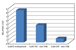
Figure 11 Cost comparison to produce GaN devices.
The use of silicon on the other hand allows vendors to move to larger diameter fabs with typical volumes greater than 5,000 8-inch wafer starts per week. Here CMOS process control typically enables line yields that are above 98 percent. Because of the extreme high volume of the end markets that CMOS is addressing, balancing yield and cost dynamics is critical, and this drives a level of operational discipline that is not available in the III-V industry.
At full maturity, the GaN on Si cost structure in mainstream silicon fabs could be reduced significantly from today’s GaN on SiC structure. As shown in Figure 11, scaling GaN from small diameter GaN development fabs to 200 mm silicon fabs achieves an almost 10 times reduction in cost. This cost advantage is further multiplied by the very high volume of a CMOS facility and could reach a 100 times reduction in total cost in the future.
To achieve significant GaN volumes at 8 inch, RF demand will be augmented with GaN on Si production that will be driven by the DC power market. This market may be as much as 10 times larger than the RF and microwave market. With upwards of 95 percent of GaN unit volume going forward tied to GaN on Si, both the DC power and RF domains will likely be serviced by the same 8 inch silicon fabs.
To fully realize the commercial promise of GaN, there must also be surety of supply to promote stability and resiliency – to say nothing of economic efficiency – across the GaN supply chain. Dual-source support is a key requirement for high volume, risk adverse applications.
Advanced Packaging
GaN supply chain optimization will be driven in parallel by process efficiencies and customer demand, the alignment of which will ultimately yield significant cost reductions for all involved. Manufacturing efficiency gains drive reduced production and product costs, which drive volume demand, and so on. But system designers in the RF and microwave domain are of course no strangers to these dynamics, having already seen this evolution in previous technology deployments.
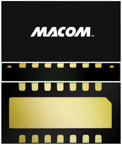
Figure 12 Typical plastic DFN package (3 × 6 mm) used for GaN devices.
A plurality of packaging options, that support end market applications, is the next critical performance and cost factor which must be considered for a complete product solution. Developments have led to the adoption of organic packaging technologies into RF, microwave and millimeter wave applications, extending the functionality and frequency of performance of plastic packaged parts. Recently, MACOM has focused on the introduction of surface mount plastic packaging for high power devices. Plastic packaged high power GaN enables designers to adopt conventional surface mount manufacturing approaches that lead to system size and weight reductions. In this way, the adoption of GaN in plastic facilitates system manufacturing cost reduction together with test efficiencies associated with high volume plastic packaging. The arrival of GaN in plastic devices has given system designers newfound flexibility to reach power levels up to 90 W without the size or weight penalties typically associated with packaged transistors (see Figure 12).
GaN on Ceramic remains the packaging option of choice for devices that must be hermetically sealed in order to ensure reliable operation in environmentally challenging conditions. Ceramic-packaged GaN devices are also capable of managing much greater power output levels than plastic-packaged alternatives available today.
When measuring the value/useful applicability of ceramic- versus plastic-packaged GaN transistors, the target lifecycle for the end system is often the deciding factor. Military radar system designers have higher expectations for environmental ruggedness than designers of many consumer products. Ceramic-based GaN devices are ideally suited for systems that are expected to deliver extremely high reliability for long periods of time with minimal maintenance, and are often less sensitive to cost pressures than commercial-caliber systems.
Conclusion
GaN on SiC is well suited for high performance RF applications but GaN on Si is well suited to most commercial and some military applications that are cost sensitive and where the performance of GaN on Si meets its needs. As GaN on Si scales up and uses larger diameter Si fabs, it will have a cost structure low enough to broadly replace many incumbent technologies in a wide range of applications. Just as one can leverage high volume silicon fabs to achieve low cost structures for compound semiconductors, one can leverage packaging and production efficiencies – also enabled by silicon – to help achieve the mainstream commercialization of GaN technology.