
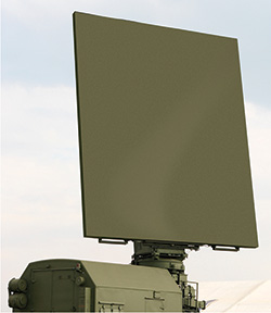
Figure 1 The active phased array architecture enables the beam to be electronically steered and multiple radars to be combined in a single system.
Editor’s Note: This month’s theme of radar and antennas features two articles discussing architectural changes that are accelerating the evolution to the next-generation of phased array radar. The first, by Doug Carlson of MACOM, discusses the development of a tile array built with commercial manufacturing processes. This approach yields a system that can perform multiple radar functions with a single aperture, at a cost lower than the traditional slat array. MACOM and MIT Lincoln Laboratory are developing this scalable tile array for the next generation of weather and air traffic control radar. The second article, by Peter Delos of Analog Devices, discusses how the continuing evolution of semiconductor and packaging technologies is enabling digital beamforming at every element in the array — through S-Band today, to X-Band in the not-too-distant future. Digital beamforming promises improved system performance, greater flexibility and lower cost.
Defense and civil radar infrastructure has historically evolved over lengthy cycles, fueled by massive investments of time, innovation and capital. Defense applications have been chiefly responsible for driving this development, yielding significant radar performance improvements, often with concomitant increases in total system cost. These initiatives have catalyzed the transition from conventional, mechanically-steered radar architectures to active electronically scanned array (AESA)—or active antenna array— that enable huge gains in temporal and spatial precision, leveraging advanced multi-beam capabilities. AESAs’ multi-function capability is similarly compelling, affording newfound agility to consolidate disparate radar systems onto a single platform (see Figure 1).
The performance characteristics of AESAs position this technology as the clear successor to legacy defense radar systems, and AESA implementations are already well underway in this domain. Deployable across ground, sea and air, AESA technology dramatically strengthens the sensor mesh network and improves situational awareness throughout the modern battlefield. Propagated to civil radar infrastructure, AESAs have the potential to profoundly affect the safety and security of citizens. A single network of multifunction AESA radars can improve air traffic control, providing direct economic benefit to the country and bolstering homeland defense capabilities, while simultaneously dramatically improving weather surveillance. With AESA technology, meteorologists can better predict and assess severe storms and save lives. AESAs will also provide the sensor capability that will bring drones and unmanned vehicles into the mainstream. This will transform society, fundamentally altering transportation and commerce.
For AESAs to successfully transition from defense to civil and commercial applications, however, there are technical and economic hurdles to overcome. Continued reliance on conventional RF components and cumbersome assembly techniques, among other factors, has blocked the path to mainstream adoption. To gain a perspective on where this development activity is headed, it’s helpful to understand its origins and roadmap to date.
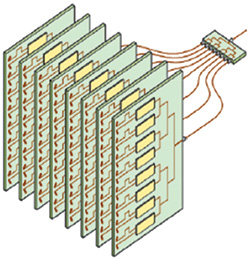
Figure 2 Slat array.
R&D ROADMAP
Next-generation active antenna technology has its roots in development programs dating back to the 1960s. With the maturing of GaAs monolithic microwave integrated circuit (MMIC) technology in the 1980s, AESA development accelerated. The U.S. Defense Advanced Research Projects Agency (DARPA) worked in partnership with MACOM and other technology companies on the Microwave/Millimeterwave Monolithic Integrated Circuits (MIMIC) program and then the Microwave Analog Front End Technology (MAFET) program. These initiatives helped advanced compound semiconductor technologies make the leap from laboratory research to commercially manufactured RF devices, yielding the industry’s first multi-watt MMICs. Further development of these semiconductor and packaging technologies led to the first mass-produced RF modules and components to use mainstream printed circuit board (PCB) technology and surface mount assembly techniques. This activity was followed by DARPA programs aimed at developing compound semiconductors for higher output power, higher efficiency and higher frequency operation. GaN technology became a major focus of development and investment, culminating with high frequencies (to 500 GHz), yield, uniformity and reliability.
Initiated in 2014, DARPA’s Arrays at Commercial Timescale (ACT) program is designed to streamline development and manufacturing cycles for next-generation radar, electronic warfare (EW) and communications systems by leveraging best practices established in the commercial domain. It aims to achieve a digitally-interconnected phased array building block, from which larger systems can be built without a full redesign for each new application. This approach to radar system implementation is anticipated to shorten time-to-market and reduce costs, both necessary for AESAs to achieve mainstream adoption for civil and commercial applications.
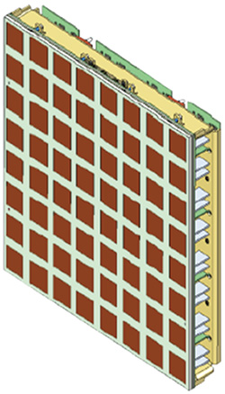
Figure 3 Tile array.
SLAT vs. TILE
The cost and mainstream viability of AESAs correlate to the cost of the electronic components that comprise them and the way they are architected in the array. From the transmit/receive (T/R) module to the RF boards and cabling, there are many considerations to weigh that impact final system cost.
Approximately half the cost of the phased array portion of the radar is attributable to the T/R module, the cost of which is determined by the types of MMICs, housing and substrates used in the module. Conventional T/R modules for radar applications employ ceramic-based materials for the substrates and are manufactured using chip-and-wire assembly processes, during which MMIC die and other ICs require additional touch labor. These add considerable expense compared to plastic encapsulated MMICs used in commercial systems. The multi-layer RF boards and cables employed in the phased array design account for almost all the rest of the cost (assembly and test processes and the structure represent approximately 10 percent of the total cost). As with the T/R modules, the underlying architecture of the array design can add considerable cost.
This is exemplified via the conventional approach to constructing large phased arrays, commonly known as the slat array architecture, which has a series of slats arranged perpendicularly to the face of the array (see Figure 2). The slat approach has a couple of advantages: it provides a large surface area on which the T/R modules and supporting components can be attached. Also, the thermal load from the high power amplifiers can be distributed across a large volume, factoring in the depth of the slat and the aperture area. The downside is that a large number of RF boards and copious cabling are required to channel the RF, DC and control signals on and off the slats. This adds considerable cost to the design.
An alternative approach—the tile array—overcomes these disadvantages through a more streamlined architecture, where the array is constructed of layers that are oriented parallel to the face (see Figure 3). Antenna elements and RF beamformers are integrated in a single, multilayer RF board, with the T/R modules mounted on the back of the board. This approach significantly reduces the area of the RF boards and dramatically reduces the number of cables and connectors. Costs can be further reduced through the use of T/R modules designed to leverage volume-scale commercial packaging and manufacturing techniques. With this approach, the T/R module MMICs are assembled in industry standard, quad flat, no-lead (QFN) packages that are directly soldered onto an inexpensive PCB that is soldered to the back of the tile. Simple metal pads lining the edge of the PCB serve as the RF and DC interconnects between the T/R module and the back of the tile.
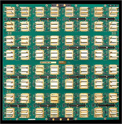
Figure 4 SPAR™ Tile prototype developed by MACOM and MIT Lincoln Laboratory.
Comparing the relative transmit power per unit area versus the cost per unit area for the slat and tile array architectures, a greater than 5x cost reduction can be achieved with the tile array at both high power and low power outputs.1
MULTIFUNCTION RADAR
Working together, MACOM and the Massachusetts Institute of Technology (MIT) Lincoln Laboratory have optimized the tile array architecture, demonstrating the cost efficiencies that can be achieved using commercial manufacturing processes. Sponsored by the Federal Aviation Administration (FAA) and National Oceanic and Atmospheric Administration (NOAA), the MACOM/Lincoln Laboratory Multifunction Phased Array Radar (MPAR) is designed to be the next-generation civil radar, integrating eight separate legacy radar functions into a single multifunction platform. The first-generation MPAR (see Figure 4) uses an array of Scalable Planar Array (SPAR) Tiles to detect and track weather systems, aircraft and airborne objects.
While most legacy radar systems mechanically rotate and tilt the radar dish to scan different sectors of the airspace, the SPAR™ Tile-enabled radar comprises hundreds to thousands of T/R elements in a stationary flat panel array that electronically scans the airspace. As shown in Figure 5, the MPAR SPAR Tile consists of a front aperture printed circuit board (APCB) containing the radiating elements, transmit and receive beamforming networks, power and logic distribution. The T/R modules are surface-mounted to the back of the APCB using standard industry manufacturing processes. A second PCB, the backplane, contains the DC power supplies, general purpose processors and high level logic. It is combined with the APCB to form the SPAR Tile. The two PCBs are connected with low cost, high performance interconnects, and a simple mechanical structure holds the two PCBs together and forms the structure for the assembly of the full array.
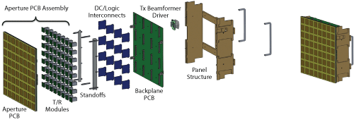
Figure 5 SPAR Tile construction.
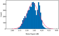
Figure 6 Noise figure distribution of the ATD T/R modules. The histogram approximates a normal distribution with a mean noise figure of 3.7 dB.
The first deployed MPAR prototype is being validated for weather observation by the National Severe Storms Laboratory (NSSL) in Oklahoma. It also provides a baseline platform for the development of backend architecture and AESA data-driven weather modeling algorithms. When fully implemented, this system will help increase forecast accuracy for severe weather events such as tornadoes, enabling earlier major storm warning and other benefits. For the FAA, MPAR systems can dramatically improve air traffic awareness and homeland defense surveillance.
MACOM has been maturing the SPAR Tile technology for almost a decade. From concept demonstration to the deployment of the first prototype system in a realistic end-use environment, the Technology Readiness Level (TRL) and Manufacturing Readiness Level (MRL) of the SPAR Tiles have advanced. Based upon the success of the first prototype system, MACOM has begun the first phase of scaled manufacturing of SPAR Tiles, with over 90 tiles for the FAA/NOAA Advanced Technology Demonstrator (ATD) being delivered for a full system demonstration. This has allowed, for the first time, meaningful statistics to be gathered on the performance distribution from the end-to-end manufacturing process. Over 6,000 T/R modules have been built and tested, yielding data such as shown in Figure 6.
TILE-BASED AESA OPPORTUNITIES
With legacy civil radar infrastructure for air traffic control and weather surveillance approaching the end of life and government-mandated spending reductions impacting key defense programs, there is a unique opportunity to develop a new and more cost-effective approach to radar system production, an approach combining an innovative RF system architecture with commercial manufacturing processes.
Tile-based AESAs create the foundation for such a new generation of high performance, agile radar systems that can be built quickly and cost effectively and flexibly tailored and scaled for deployment across defense, civil and commercial applications. The design and assembly techniques used for the tile array MPAR address both communications and sensing applications, enabling active antenna capability at a cost point that makes this technology viable for a wide range of commercial use cases: internet in the sky, 5G, sense-and-avoid for airborne drones and radar for autonomous vehicles.
Reference
- Jeffrey S. Herd and M. David Conway, “The Evolution to Modern Phased Array Architectures,” Proceedings of the IEEE, 2016, Vol. 104, Issue 3, pp. 519–529.