
A culture of continuous innovation in the consumer electronics industry has conditioned us, as consumers, to expect technology improvements at rates that are faster than ever before. Not only are these products becoming more complicated, but increasing competition has dramatically reduced the typical design cycles. As a result, the ability of an engineering organization to move a product from schematic to final product through efficient design and test practices has become a competitive advantage.
Although improvements in development practices can often require organizational change, there are several practical tips that engineers can implement to ultimately reduce time-to-market. In this article, everything from simple design choices for better manufacturability to careful planning of test software and hardware will be discussed. Three of the most critical best practices include:
- Design for manufacturability and debugging
- Writing scalable and reusable test code
- Replicating the physical manufacturing environment in all stages of development
In order to understand best practices for taking a product from design to test, one must consider that manufacturing test goals are often quite different from the goals of design verification. Design verification testing is meant to verify that the product meets its specifications under all operating conditions. By contrast, manufacturing test is designed to ensure that the product was assembled correctly with all components functioning as expected. In spite of the differences between these goals, engineers can leverage verification testing development in manufacturing with careful planning. Note that although the best practices described here are specifically applied to RF product developent, the philosophies presented apply to any type of commercial product design.
Design for Manufacturability
In many organizations, development groups often do not consider manufacturing test until the very end of a design cycle. However, in order to properly leverage design efforts for manufacturing, designers must anticipate manufacturing test issues from the very first revision of the design. Many times, if consideration is given for manufacturing test early in the design process, important decisions on layout and access to test signals/circuitry can reduce the overall cost of validation and manufacturing test.
For example, many times it is difficult to include control circuitry such as highly integrated ASICs in initial revisions of a product. This results in the need for expensive test equipment that emulates the device’s operating environment – leading to longer and more costly test times. As an example, the lack of non-signaling modes on cellular chipsets can substantially increase product validation times. Without non-signaling modes in the initial revision of a product, engineers are forced to test the radio with more expensive and substantially slower base station emulators. Thus, by including critical control circuitry in initial revisions of a product, engineers can frequently reduce validation time through the use of less expensive test equipment such as a signal generator and signal analyzer.
One of the simplest ways to reduce potential issues in manufacturing is to strictly adhere to design rules such as: component spacing, “keepout zones,” and proper pad shapes to prevent component “tombstoning.” Both PCB and chip-level manufacturers frequently provide design rule checking software to ensure that the design can be practically manufactured. Following these design guidelines from the very first layout is extremely important. Although designers are often tempted to “fudge” design rules until later revisions, the delay often makes the changes even more difficult to implement. On the other hand, engineers considering design rules on the first revision will result in a much more robust design and easier transition to manufacturing.
Probing and Debugging
One practical tip to identify manufacturing issues in complex designs is to use appropriate debugging and test interfaces. Engineers can generally improve their ability to test or debug or troubleshoot a circuit through two primary methods. First, it is important to design probe pads and various test interfaces into the product itself. Second, engineers should develop production-grade test fixturing in parallel with the initial design to ensure more repeatable validation measurements.
In development, engineers frequently use manual probes to troubleshoot problems with a circuit. However, manual probes are subject to measurement error and can lead to incorrect assumptions about circuit performance. In both design and manufacturing, it is often essential to provide detailed insight into the performance of a product. Thus, designers must consider adding the ability to probe a design in a way that is repeatable and has minimal impact on the impedance of the circuit. Considering probing needs early in a design cycle enables engineers to ensure the circuit layout and component placement allows for proper probing.
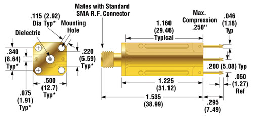
Figure 1 Schematic of an Everett Charles Coaxial Probe.
Engineers are often reluctant to use inter-board connectors due to the cost. Probes can be a viable solution provided one gives attention to the attenuation and uses the proper probe and landing pattern. For low frequencies (below 100 MHz), designers frequently use “pogo”-type probes to measure signals on specific PCB traces. These probes are named for their spring-loaded mechanical action (like a pogo stick) and are very effective when used with the appropriate probe pad. At RF frequencies, however, pogo-type probes and the associated landing pads are susceptible to a host of high frequency related parasitic behavior that can impact electrical performance such as impedance match and insertion loss.
There are several probing solutions at RF and microwave frequencies, and one that we have found to be particularly effective is the use of broadband coaxial probes. Coaxial probes, such as the Everett Charles K-50L (see Figure 1), feature an SMA connector for easy connectivity to a spectrum analyzer or power meter. Although probes and probe landing pads are useful in many instances, RF engineers are often reluctant to use probe pads since they can lead to destructive capacitance and degrade circuit performance. One frequent workaround is to design the probe pads from the actual board traces. For example, if the designer knows he will be using an RF probe, the board geometry (such as trace width and ground plane spacing) can be designed to accommodate this probe without the need for specific landing pad geometries. In some instances, one can use surface mount component pads to double as a probe pad, allowing one to probe the circuit in a well-matched interface with the component removed.
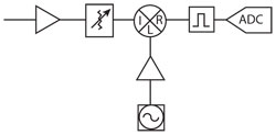
Figure 2 Typical receiver architecture.
Another effective solution for both validation and manufacturing test is to use a coaxial connector with an integrated switch. In this approach, the mechanical action of connecting a probe drives a single-pole double-throw switch. Thus, the switch will internally route to one terminal when the probe is not connected, and a second terminal when the probe is engaged. The integrated connector/switch probes were initially designed for the cellphone industry as a means to measure RF power through a connector by disconnecting the antenna. Today, RF engineers can choose from a range of devices with excellent performance at 12 GHz and beyond.
Layout Best Practices
One important yet often overlooked consideration in design for manufacturability is isolation of key circuitry. For example, consider the block diagram of a typical receiver shown in Figure 2. In order to adequately determine the performance of individual components, the designer needs to be able to isolate the mixer from the amplifier and isolate the local oscillator from the mixer. If the synthesizer is directly attached to the mixer without any interface to separate the two components, it would be more difficult to troubleshoot potential issues with the synthesizer. By separating these interfaces and testing each section individually, one can accurately troubleshoot issues with more complex components.
There are multiple ways to separate critical interfaces. One is to physically separate the layout of each subassembly and connect them through coaxial connectors such as an SMA. Unfortunately, SMA connectors often increase size and add cost to the design. Integrated switch/connector assemblies (such as the one described earlier) provide an excellent alternative as they are a well-matched pass-through part with essentially nonexistent insertion loss.
Correlating Measurements Through Reusable Test Code
Another issue that test engineers often face is the ability to correlate manufacturing data with measured results completed during validation testing. Difficulty in correlation can occur for several reasons, including the use of different test equipment, the effect of test fixtures, and changes in the physical environment. One of the easiest issues to mitigate is the errors associated with using different measurement algorithms in validation and manufacturing test.
In general, R&D groups typically require very high performance instruments to ensure that the specification limits of the instrument do not influence the validation test results. By contrast, the sheer amount of instrumentation required for a large-scale production operation typically requires manufacturing test equipment to be cost optimized. Unfortunately, the differing requirements of validation test and manufacturing test often lead organizations to use very different test equipment – causing problems with measurement correlation and introducing additional effort to write test software.
Because differences in measurement algorithms can lead to differences in measurement results, one of the simplest steps to improve correlation between validation and production testing is to ensure that all measurements use the same measurement algorithm. One can ensure algorithm standardization through practices such as:
- Use of software algorithms that run on a PC (or PXI system) rather than a test instrument
- Use of similar test equipment (same vendor) in both validation test and production test
- Use of industry-defined measurements such as those defined by IEEE standards.
Of these, one of the simplest methods to ensuring measurement algorithm standardization is the use of instrumentation from the same vendor in all stages of product development. This approach also provides the added benefit of being able to more easily leverage test code written for validation test in the production test phase.
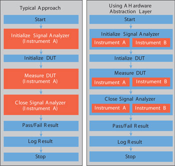
Figure 3 Traditional approach versus use of a hardware abstraction layer.
Leveraging Test Code between Validation and Manufacturing Test
Although leveraging validation test code in manufacturing might seem like an obvious best practice, it requires careful attention to software architecture. For example, using a modular and hierarchical software architecture is critical in order to leverage validation test code in manufacturing test. When writing software for validation testing, it is often tempting to generate code in the fastest way possible – without attention to architecture or long-term supportability. However, because much of the same measurements performed in validation are also performed in production test, it is useful to ensure that the validation test code is as flexible as possible.
A simple best practice for writing test software is to use a hardware abstraction layer. The idea of this practice is to encapsulate driver calls for a particular instrument within a higher-level function call. This approach makes it easier to modify the test code in the future to add additional instrumentation without a major rewrite. As observed in Figure 3, the use of a hardware abstraction layer requires that the test code be architected such that a specific instrument’s driver calls are within the framework of a function call to the instrument family. Although it requires better up-front planning, the implementation of a hardware abstraction layer improves test code reuse and can ultimately reduce test software development time. Note that the hierarchical nature of a hardware abstraction layer is relatively straightforward in natively hierarchical programming languages such as NI LabVIEW system design software or other similar languages.
Note from Figure 3 that an important architectural practice is to separate code to configure the DUT from code to configure the instrument. Although these tasks can often be executed in parallel, it is a better design practice to ensure that the two tasks are independent of one another. In some instances where measurement speed is of the utmost importance, test executive software can automatically configure two independent function calls to execute in parallel.
Common Physical Environments in Validation and Manufacturing
The physical environment of an engineering lab is often very different than a manufacturing facility. Although it might seem counterintuitive, manufacturing environments often experience a much wider degree of variability than what is present in the lab. In addition, fluctuations in temperature, problems with power quality, and even spurious responses from other devices can affect test results. A final best practice is to ensure that the physical environment during validation testing is identical to the physical environment on the manufacturing floor.
Although a wide range of challenges in the manufacturing environment can influence a measurement result, temperature variation is one of the most problematic. On a manufacturing floor, the high density of electronic equipment can emit significant and widely varying heat radiation. In addition, simple attributes such as being located underneath an air conditioning vent or near a door can also affect the localized ambient temperature. Thus, while an ideal manufacturing facility might tightly control air temperature on a large scale, it is extremely difficult to control local temperature at the DUT. Not only do these fluctuations in temperature affect the accuracy of the instrumentation, but they also significantly affect the performance of the DUT.
In my years of manufacturing experience, I have personally observed factories where the ambient temperature was controlled to within one degree, but with up to 10 degree swings in temperature localized at a particular test station. As context to the effect of temperature on measurement quality, a typical high frequency amplifier typically experiences power variation of up to 0.03 dB per degree C. With instruments and complex devices having several amplifiers in a single signal chain – the power error associated with temperature variation can quickly stack up. Such large swings in temperature can cause substantial issues when trying to align the output power to within a tight range such as ±0.5 dB (or better) typically required for power amplifiers.
One of the best first-order attempts to reduce temperature variation due to electronic equipment is to ensure proper airflow and ventilation. In addition, it is often useful to accompany each RF measurement (either in validation or in manufacturing) with a temperature measurement. Especially in larger PCB designs, an on-board temperature sensor is a reliable method to monitor temperature. By monitoring the temperature, engineers can associate each RF measurement with the environmental conditions. As a result, the temperature data can often explain discrepancies between validation and production test results.
Fixturing
Another way to replicate the production environment in validation is to use standardized fixturing practices. In many organizations, fixturing is often ignored until the product has been transitioned into the manufacturing phase of development. Although fixturing can either enhance or degrade measurement performance, it is important to use production-quality fixturing early in the development cycle. Fixturing should be designed and manufactured in parallel with one of the early or first design revisions.

Figure 4 Board-level validation and manufacturing test fixture.
In the characterization environment, it is common for engineers to test designs using poor cabling solutions such as flimsy cables and low-quality connectors that are difficult to de-embed. The use of high-quality fixturing, traditionally reserved for production test, has several benefits. First, using fixturing in validation testing improves this measurement quality by making them more repeatable and stable. Second, and perhaps more importantly, the use of better fixturing during validation often helps one to better correlate validation test results and manufacturing test results. An example of a board level fixture is shown in Figure 4.
Production quality fixturing also enables engineers to test a DUT with little direct operator interaction. Typical production-grade fixtures provide repeatable interfaces for both RF/analog measurements, control I/O and DC power. In addition, fixtures can also protect from important environmental aspects such as electromagnetic interference, and better heat dissipation. Fixtures also minimize touch from human hands – which can also affect the quality of the product.
Electromagnetic Emissions
A final method to ensure common physical environments between validation and manufacturing is to measure and, if necessary, compensate for the electrical environment. In general, validation labs are relatively electrically quiet. With fewer products being tested and less electronic equipment than in a manufacturing environment, the lab contains a relatively small number interference producers. In some instances, well-shielded enclosures in the validation lab protect a DUT from outside spurious emissions.
When performing validation testing, an important best practice is to duplicate the manufacturing environment in the lab. For example, one can use a spectrum analyzer to measure radiated electromagnetic spurs, and then use other DUTs to re-create the effect in the validation lab. Other conditions that are useful to replicate include power supply variations. Power supply analysis is especially useful when using manufacturing facilities in locations where power stability is more problematic. By emulating the manufacturing environment during validation testing, one can predict their test system robustness and also determine the impact to test limits. This type of investigation can prevent crisis management on test issues that could occur during early production runs.
Conclusion
As the electronics industry has evolved to become more competitive, it is increasingly important for organizations to adopt practices enable them to move products from design to production test more quickly. As this article discusses, engineers must become increasingly aware of design for manufacturability, test code development, and the conditions of the manufacturing environment. Taking these areas into account early on in a design will allow for a much-improved efficiency to transition the product to production.
Bill Reid is a chief hardware architect at National Instruments with 29 years of experience in the RF/microwave industry. He has extensive expertise in micrpowave product design, developing manufacturing test systems, consulting with customers, and general management. During his 12 years at NI, he has served both a business and technical leader. Along with his system and board-level design experience, Reid also has extensive metrology experience, developing the calibration routines and accuracy models for NI’s RF products. Prior to NI, Reid worked at General Dynamics, EG&G, Texas Instruments and Nokia Mobile Phones. Reid has a bachelor’s degree of electrical engineering from the University of Illinois at Chicago and graduate studies at California State University, Fullerton