
Recently, multi-layer LTCC technology has been used extensively for the miniaturization of RF passive components and antennas. In addition to the high integration by embedding components and interconnects, high Q passive elements have been demonstrated with LTCC technology.1 It is suitable to integrate antennas and other passive components, even with active devices. Higher integration and more compact structures make LTCC technology popular in RF applications.
A chip antenna using LTCC technology for 2.45 GHz applications has been reported.2 Another chip antenna, using meander lines mounted on LTCC chip, has a wide bandwidth (19.1 percent at VSWR < 2) at 1800 MHz.3 Because these planar meander lines are deposited on the surface of the LTCC chip, their size is larger than that with embedded meander lines. In this article, LTCC technology is used to develop a 900/1800 MHz dual-band chip antenna. The multi-layer printed helical-monopole antenna structure is designed to obtain the dual-band function. The HFSS 3-D EM simulator, based on the finite-element method, is employed for design simulation. Simulation results are compared with the measured performance and discussed.
Dual-band Antenna Design
| |||||||
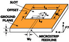
A helical-monopole combination structure for GSM 900/1800 MHz has been proposed for dual-band antenna designs.4 Figure 1 shows a dual-band helical-monopole combination antenna, a multi-layer printed helical-monopole LTCC chip antenna and the geometry of a LTCC chip antenna mounted on a FR-4 substrate board. A cross section of the printed helical structure, realized by using via holes to connect upper- and lower-layer metals, is shown in Figure 2. The printed monopole is located on the middle layer. The dielectric constant and loss tangent of the LTCC ceramic are 7.8 and 0.0047, respectively. The 3.6 mil thick top-layer ceramic is placed above the upper-layer metal. The thicknesses of the other layers are also shown. The dimensions of the LTCC chip and each layer are converted from the free-space helical-monopole antenna to the multi-layer ceramic based on its dielectric constant.
| |||||||

The first monopole antenna, as shown in Appendix A, contributes to the higher frequency (1800 MHz) band. The helical antenna is tuned to the lower frequency (900 MHz) band. In the initial design, the input impedance of the LTCC chip antenna is capacitive, hence several closer turns of helical lines are used as an inductor for input impedance matching. In order to increase the bandwidth, three printed monopoles with different lengths are used, integrated with the helix. Figure 3 illustrates the triple resonant frequencies used to achieve a wider bandwidth.
| |||||||

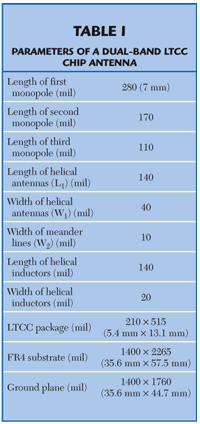
The dimensions of the LTCC chip antenna are 210 x 515 x 44.8 mil (5.4 x 13.1 x 1.14 mm). The widths of the embedded meander lines and printed monopole antennas inside the LTCC chip are all 10 mil. The dimensions of the FR-4 circuit board are 1.400 x 2.265 x 0.039 in. (35.6 x 57.5 x 1 mm) and the size of the ground plane is 1.400 x 1.760 in. (35.6 x 44.7 mm). Additional dimensions are listed in Table 1.
Simulation and Measured Results
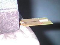
Figure 4 shows the simulated current distributions of the dual-band LTCC chip antenna at 900 MHz with different phase at 0°, 45°, 90° and 135°. The current flowing along the metal strips inside the LTCC package can be observed. Figure 5 shows the photograph of a fabricated dual-band LTCC chip antenna on a FR-4 PCB board and the simulated and measured return losses. It is observed that the measured resonant frequencies are shifted from the simulated 900 and 1800 MHz to higher frequencies, 1040 and 1900 MHz. The measured return loss, S11, is –21.8 and –20.9 dB at 1040 and 1900 MHz, respectively. The simulated and measured return losses are also listed in Table 2.
| |||||||

| |||||||||

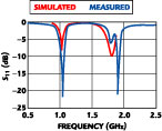
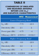
Figure 6 shows the simulated 3-D antenna patterns at 900 and 1800 MHz. They are very close to those of an ideal dipole antenna. Figure 7 shows photographs of the setup for radiation pattern measurement of the chip antenna in an anechoic chamber. Figure 8 shows the simulated and measured 2-D antenna patterns in the E-plane (XZ-plane) for the lower and higher frequency bands. Satisfactory agreements between the simulation and measurement are observed. Figure 9 shows the measured vertical and horizontal polarization patterns in the H-plane (XY-plane). The vertical-polarization patterns (H-plane) are very close to the omni-directional patterns of a dipole antenna. The measured antenna directivity is approximately 2 dBi at both the lower and higher frequency bands. The measured antenna power gains are approximately "4 and "6 dB at 1040 and 1900 MHz, respectively, which are lower than the simulated results by approximately 2 to 3 dB.
| |||||||

| |||||||

| |||||||

| |||||||

The radiation efficiency (![]() r ) of the chip antenna can be obtained from the relation between the directivity (D) and power gain (GP) in accordance with
r ) of the chip antenna can be obtained from the relation between the directivity (D) and power gain (GP) in accordance with
![]() r (dB) = GP–D
r (dB) = GP–D
![]() r (dB) = 10• log[
r (dB) = 10• log[![]() r (linear scale)]
r (linear scale)]
As shown by the data, the simulated and measured antenna efficiencies are 51.4 and 24.3 percent at the lower frequency band, and 20.6 and 13 percent at the higher frequency band, respectively. The difference between the measurement and simulation results for the radiation efficiency of the LTCC chip antenna, which is about 2 dB lower, may be due to the loss in the manufacturing process of the LTCC chip.
Conclusion
The design simulation, fabrication and measurement of a 900/1800 MHz dual-band chip antenna using LTCC multi-layer technology is presented. The helix-monopole structure is used to obtain dual-band characteristics. The Ansoft HFSS 3-D EM simulator is used for the design simulation. Satisfactory agreement between simulated and measured results on antenna patterns has been achieved. The measured return losses (S11) are –21.8 and –20.9 dB at 1040 and 1900 MHz, respectively. The vertical-polarization patterns (H-plane) are very close to the omni-directional patterns of a dipole antenna. The measured antenna power gains are approximately –4 and –6 dB at 1040 and 1900 MHz, respectively, which are lower than the simulated results by about 3 dB. The lower gain may be due to the loss in the manufacturing process of the LTCC chip. The measured antenna efficiencies are 24.3 and 13 percent at the lower and higher frequency bands, respectively. In order to meet the requirements for GSM/DCS applications, correcting the frequency response and increasing the bandwidth are the goals for continuing the study.
Acknowledgment
The authors would like to thank the Computer and Communication Laboratory (CCL) of the Industrial Technology of Research Institute (ITRI), Taiwan, ROC, for its support of this project.
References
- J.W. Sheen, "LTCC-MLC Duplexer for DCS-1800," IEEE Transactions on Microwave Theory and Techniques, Vol. 47, No. 9, September 1999, pp. 1883–1890.
- Y. Dakeya, T. Suesada, K. Asakura, N. Nakajima and H. Mandai, "Chip Multi-layer Antenna for 2.45 GHz Band Application Using LTCC Technology," IEEE International Microwave Symposium Digest, 2000, pp. 1693–1696.
- W. Choi, S. Kwon and B. Lee, "Ceramic Chip Antenna Using Meander Conductor Lines," Electronics Letters, Vol. 37, 2001, pp. 933–934.
- P. Haapala, P. Vainikainen and P. Eratuuli, "Dual Frequency Helical Antennas for Handsets," IEEE 46th Vehicular Technology Conference, Vol. 1, 1996, pp. 336–338.
Chi-Chang Lin received his BSEE degree from the Tatung Institute of Technology, Taipei, Taiwan, and his MSEE degree from Tatung University, Taipei, Taiwan, in 1999 and 2001, respectively. He is currently working toward his PhD degree in electrical engineering at National Cheng Kung University, Tainan, Taiwan. His research interests include EM simulation and microwave antenna design.
Yu-Jui Chang received his MSEE degree from National Cheng Kung University, Tainan, Taiwan, in 2002. He worked on chip antenna design and HBT MMIC for his master study. He is currently with ELANsat Technologies Inc. as an R&D engineer. His research interests include RF circuit and antenna design for wireless communication systems.
Huey-Ru Chuang received his BSEE and MSEE degrees from National Taiwan University, Taipei, Taiwan, in 1977 and 1980, respectively, and his PhD degree in electrical engineering from Michigan State University, East Lansing, MI, in 1987. From 1987 to 1988, he was a post-doctoral research associate at the Engineering Research Center, Michigan State University. From 1988 to 1990, he was with the Portable Communication Division of Motorola Inc., Ft. Lauderdale, FL. He joined the department of electrical engineering at National Cheng Kung University, Tainan, Taiwan, in 1991, where he is currently a professor. His research interests include antenna and RFIC/microwave circuit design for wireless communications, computational electromagnetics and applications, EMI/EMC, microwave communication and detection systems.
Appendix A
