
Defected ground structures (DGS) etched in the metallic ground plane of microstrip lines, also known as photonic bandgap (PBG) structures, are attractive to obtain unwanted frequency rejection and circuit size reduction. Research on the PBG was originally carried out in the optical regime1,2 and has recently started with DGS in the microwave field.3 Various shapes of DGS cells, such as rectangular,4–6 square,7,8 circular,9 dumbbell10–12 and combined structures13–16 have appeared in the literature. Since DGS structures have an inherent resonant property, many of them have been applied to filter circuits.5,6,11,17,18 Among the published articles, rectangular6 and dumbbell11 shaped DGSs have been applied to low pass filters.
When designing a filter, including a LPF, an elliptic function type of slope in the transition from passband to stopband is desirable. To obtain this property in a microstrip environment more effectively, a periodic or array configuration of DGS cells has been used. However, this approach makes size reduction difficult.
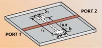 | |||
| Fig. 1 The I-shaped DGS cell structure. | |||
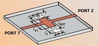 | |||
| Fig. 2 Stub-I type cell structure. | |||
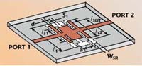 | |||
| Fig. 3 The proposed quasi-elliptic function LPF circuit structure. | |||
A fine stopband tuning characteristic, to reject harmonic and spurious signals, is another consideration in designing a filter, especially for LPFs such as IF filters for downconverters and bias circuits of oscillators and amplifiers. In conventional DGS structures, this property has been realized with the frequency variation of the stopband determined by the DGS dimensions. However, the frequency variation as a function of the electrical dimensions has not been small enough for fine-tuning and the precise design process for rejecting harmonic and spurious signals has been difficult.
In this article, the above two problems are overcome by introducing a combined structure. The structure has been developed by following three steps. In the first step, the conventional dumbbell-shaped DGS has been modified into an I-shaped DGS, as shown in Figure 1. The frequency control of the I-shaped DGS is accomplished by adjusting the length of the transverse slot (longer than that shown in Ahn11) and the dimensions a and b, which are different. The frequency control of the conventional dumbbell-shaped DGS11 had been achieved by adjusting the total area of the DGS, with the a and b dimensions identical and fixed. In the second step, a cross-junction open stub is added right above the I-shaped DGS. This structure is called a stub-I type, as shown in Figure 2. In the third step, to develop the LPF, a stub-I type DGS is placed between two identical rectangular DGSs and cross-junction open stubs, as shown in Figure 3.
Similar to the way all the previous DGS filters were designed to obtain a wide frequency stopband, in this LPF, suppression of an uprising slope at frequencies higher than the resonant frequency was pursued. The characteristics of the LPF structure will be compared with those published by D. Ahn, et al.,11 in terms of steepness of slope and stopband tuning capability, including attenuation and bandwidth. The comparison will demonstrate that this approach provides a steeper slope and a finer stopband tuning capability.
Finally, the circuit size reduction problem will be addressed. Since the study did not adopt a periodic or array configuration of DGS cells, considerable circuit size reduction, less than one fifth, has been achieved when compared to the size of a conventional stepped impedance LPF having an identical cutoff frequency of 2.665 GHz. When compared to Ahn,11 this work shows that at least a 25 percent reduction has been achieved.
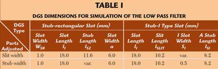
Structures and Characteristics of the Proposed DGS Cells
 | |||
| Fig. 4 I-shaped DGS cell frequency response as a function of S1 for LSLIT = 10.2 mm. | |||
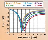 | |||
| Fig. 5 I-shaped DGS cell frequency response as a function of LSLIT for S1 = 0.5 mm. | |||
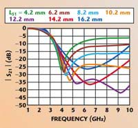 | |||
| Fig. 6 Frequency response of the stub-I type DGS cell as a function of LS1 with a = 6 mm, L1 = 20 mm, S1 = 0.5 mm and LSLIT = 20 mm. | |||
Two different microstrip DGS cell structures are first introduced for fine tuning of the stopband frequency and precise realization of the circuit configuration. The first DGS structure has an I-shaped slot etched in the ground plane. This structure can be thought of as a modified structure of the dumbbell-shaped DGS.10–12 Actually, this cell has a longer transverse slot length than that of the dumbbell type. The width, a, and the length, lI, are both normally fixed depending on the operating frequency. The length, lSLIT, and the width, SI, are adjusted for the desired properties.
The I-shaped DGS cell has been characterized with lSLIT set at 10.2 mm and SI adjusted from 0.5 to 3.5 mm with a = 6 mm and lI =18 mm. In this case, the |S21| characteristics for a frequency range from 1 to 10 GHz have been obtained, as shown in Figure 4. The slope of |S21| frequencies above the resonance is decreased for wider stopband or low pass filter property, where the resonant frequencies are changing very slowly.
Next, lSLIT was adjusted from 12.2 to 2.2 mm with SI = 0.5 mm. The frequency response for this case is shown in Figure 5. This structure provides not only a fine-tuning capability of the resonant frequency by adjusting the width SI of the center slot, but also a steep slope for frequency rejection by varying the length lSLIT. Another advantage of the I-shaped DGS is that the resonant frequency can be adjusted without modification of the circuit size.
The second circuit type is the stub-I type DGS structure, where an open stub is added right above the I-shaped slot. The reason why the stub has been added is to obtain a wider stopband with a steep slope at frequencies below the resonant frequency. To accomplish this aim, the I-shaped DGS has the following dimensions: a = 6 mm, lI = 20 mm, SI = 0.5 mm and lSLIT = 20 mm. The |S21| frequency response has been obtained with lSIM varied from 4.2 to 16.2 mm. The |S21| frequency response from 1 to 10 GHz is shown in Figure 6, where the stopband characteristics above the resonant frequency have been improved in terms of low pass filtering property by increasing lSI. The best stopband characteristic has been obtained when lSI was slightly smaller than lSLIT.
Finally, a cross-junction open stub right above a rectangular-shaped DGS cell is considered. It is called the stub-rectangular type. Since it is known that a stub-rectangular type DGS cell has a flat passband characteristic for LPF and a wide stopband property,19 and that the stub-I type DGS cell has a steep slope between pass and stopbands and a wide stopband property, the stub-I type DGS structure has been inserted between two identical stub-rectangular type structures, where the spacing between slots, d = 0.5 mm, was used since this dimension was the minimum realizable distance.
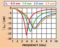
The structure has been analyzed with HFSS (High Frequency Structure Simulator, a commercial software tool based on the 3-D finite element method) with the dimensions listed in Table 1, except for SI, which has been adjusted from 0.5 to 3.5 mm. The frequency response of this structure from 1 to 10 GHz has been obtained and is shown in Figure 7, where a quasi-elliptic function slope has been demonstrated and the cutoff frequency at 2.665 GHz has been shown. When SI was between 0.5 and 1.5 mm, the sharpest cutoff slope was obtained. A wide stopband from approximately 3 to 10 GHz was also adjusted.
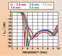 | ||
| Fig. 7 Frequency response of the LPF circuit structure as a function of S1 with the other parameters shown in Table 1. | ||
 | ||
Measurements and Comparison
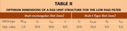
In the simulation, an LPF with a steep cutoff slope characteristic and a fine stopband tuning capability was obtained by varying the transverse slot length of the I-shaped DGS and the width of the cross-junction open stubs located above the rectangular-shaped DGS. The proposed structure has been designed and fabricated for an LPF having a cutoff frequency of 2.665 GHz and stopband peaks at 3 and 4.2 GHz, where 4.2 GHz is the second harmonic frequency for the highest passband frequency. The optimum dimensions are listed in Table 2. The LPF structure has been realized on a 9 x 18 mm Teflon substrate, as shown in Figure 8.
 | ||
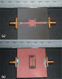 | |||
| Fig. 8 The realized LPF structure; (a) circuit side and (b) ground side. | |||
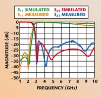 | |||
| Fig. 9 Comparison between measured and simulated S-parameters of the LPF. | |||
The S-parameter characteristics of the LPF have been measured in a frequency range from 1 to 10 GHz, and compared with the simulated results. The 0.115 to 0.127 dB insertion loss in the passband below approximately 2.1 GHz and cutoff frequency at 2.665 GHz was measured with an HP8510C network analyzer. The first attenuation pole occurred at approximately 3 GHz. This agrees well with the simulated result. The measured |S11| characteristics also agree well with the simulation results for the whole frequency range except for some deviations below 2 GHz. However, the measured |S21| shows some deviations from the simulated results at frequencies above 3.5 GHz. Even though the deviation can be more than 5 dB difference between the stopband characteristics of the measured and simulated results, they follow the same trend.
The steepness of the slope between passband to stopband of the LPF has been compared with that of Ahn.11 The slope in this study shows around 40 dB attenuation over the frequency range from 2.5 to 3 GHz, as shown in Figure 9, but the slope in Figure 14 of Ahn11 shows around 30 dB attenuation over the frequency range from 1.5 to 5 GHz. This comparison confirms that the microstrip LPF in this study has a considerably improved steepness characteristic.
In Ahn,11 an approximately 2.3 GHz resonant frequency variation has been observed for a 1.2 mm change of the slot width. However, in this study, a 2 mm change in the slot length of the I-shaped DGS gives a resonant frequency change of less than 200 MHz. This comparison shows that the proposed structure provides a much finer tuning capability than that of Ahn.11
To test the circuit size reduction effect, the circuit size of this LPF has been compared with that of a conventional stepped impedance LPF having the same cutoff frequency of 2.66 GHz (at 3 dB) as this LPF and two LPF structures proposed by Ahn.11 To evaluate how much size reduction of this LPF circuit can be accomplished, a conventional stepped impedance microstrip LPF circuit (32.16 x 28.55 mm) has been designed and simulated by HFSS with a substrate similar to the one used by this LPF. This LPF circuit (9 x 18 mm) has been realized in approximately 18 percent of the stepped impedance LPF circuit area, and in approximately 62 and 75 percent of the circuit areas T-junction (15 x 17.4 mm) and cross-junction (14.4 x 15 mm) shown in Ahn,11 respectively. Figure 10 shows the conventional stepped impedance LPF configuration and its performance.
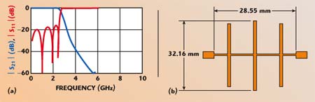 | ||
| Fig. 10 Conventional stepped impedance LPF with a 2.66 GHz cutoff frequency; (a) S-parameters and (b) circuit configuration. | ||
Conclusion
A microstrip structure is proposed, which combines a rectangular- and an I-shaped DGS with cross-junction open stubs placed right above the DGSs to obtain a steep slope characteristic and a fine stopband tuning capability. The properties of this structure have been demonstrated and compared with a conventional DGS LPF. The structure proposed shows a considerable improvement in steepness of the attenuation slope over that in Ahn.11 Thus, the LPF can be considered as a quasi-elliptic function LPF.
Since conventional DGS structures have been usually realized in an array or periodic form to obtain the above performance, circuit size reduction was very difficult. Achieving a fine frequency tuning of the stopband characteristics to reject harmonic and spurious signals of IF filters for downconverters and bias circuits of oscillators and amplifiers has been difficult with DGS structures. These problems for a LPF have been overcome in this study.
This approach leads also to a circuit size reduction. This LPF circuit (9 x 18 mm) has been realized in approximately 18 percent of the stepped impedance LPF circuit area, and in approximately 62 and 75 percent of the circuit areas in T-junction (15 x 17.4 mm) and cross-junction (14.4 x 15 mm), which appeared in Ahn,11 respectively.
Acknowledgment
This work was supported in part by Kyung Hee University.
References
- C.M. Bowden, J.P. Dowling and H.O. Everitt, “Development and Applications of Materials Exhibiting Photonic Bandgaps,” Journal of the Optical Society of America, Vol. B10, February 1993, p. 280.
- Journal of Lightwave Technology, Special Issue, Vol. 17, No. 11, November 1999.
- IEEE Transactions on Microwave Theory and Techniques, Special Issue, Vol. 47, No. 11, November 1999.
- T. Yun and K. Chang, “One-dimensional Photonic Bandgap Resonators and Varactor Tuned Resonators,” 1999 IEEE MTT-S Symposium Digest, pp. 1629–1632.
- R. Qiang, Y. Wang and D. Chen, “A Novel Microstrip Bandpass Filter with Two Cascaded PBG Structures,” 2001 IEEE AP-S Symposium Digest, pp. 510-513.
- J.P. Kim and W.S. Park, “Microstrip Low Pass Filter with Multislots on Ground Plane,” Electronics Letters, Vol. 37, No. 25, December 2001.
- M. Kahrizi, T. Sarkar and Z. Maricevic, “Dynamic Analysis of a Microstrip Line Over a Perforated Ground Plane,” IEEE Transactions on Microwave Theory and Techniques, Vol. 42, No. 5, May 1994, pp. 820–825.
- X. Yi, P. Yeh and J. Hong, “Photonic Bandgap Structure in Thin Film Waveguides,” SBMO/IEEE MTT-S IMOC ‘99 Proceedings, pp. 451–453.
- V. Radisic, Y. Qian, R. Coccioli and T. Itoh, “Novel 2-D Photonic Bandgap Structure for Microstrip Lines,” IEEE Microwave and Guided Wave Letters, Vol. 8, No. 2, February 1998, pp. 69–71.
- C. Kim, et al., “A Novel 1-D Periodic Defected Ground Structure for Planar on Circuits,” IEEE Microwave and Guided Wave Letters, Vol. 10, No. 4, April 2000, pp. 131–133.
- D. Ahn, et al., “A Design of the Low Pass Filter Using the Novel Microstrip Defected Ground Structure,” IEEE Transactions on Microwave Theory and Techniques, Vol. 49, No. 1, January 2001, pp. 86–91.
- S. Jeong, et al., “Amplifier Design Using l/4 High Impedance Bias Line with Defected Ground Structure (DGS),” 2002 IEEE MTT-S International Microwave Symposium Digest, pp. 1161–1164.
- F. Yang, K. Ma, Y. Qian and T. Itoh, “A Uniplanar Compact Photonic Bandgap (UC-PBG) Structure and Its Applications for Microwave Circuits,” IEEE Transactions on Microwave Theory and Techniques, Vol. 47, No. 8, August 1999, pp. 1509–1514.
- R. Coccioli, F. Yang, K. Ma and T. Itoh, “Aperture-coupled Patch Antenna on UC-PBG Substrate,” IEEE Transactions on Microwave Theory and Techniques, Vol. 47, No. 11, November 1999, pp. 2123–2130.
- F. Yang, K. Ma, Y. Qian and T. Itoh, “A Novel TEM Waveguide Using Uniplanar Compact Photonic Bandgap (UC-PBG) Structure,” IEEE Transactions on Microwave Theory and Techniques, Vol. 47, No. 11, November 1999, pp. 2092–2098.
- Q. Xue, K.M. Shum and C.H. Chan, “Novel 1-D Microstrip PBG Cells,” IEEE Microwave and Guided Wave Letters,” Vol. 10, No. 10, October 2000, pp. 403–406.
- J. Yun, et al., “A Design of the Novel Coupled Line Bandpass Filter Using Defected Ground Structure,” 2000 IEEE MTT-S International Microwave Symposium Digest, pp. 327–330.
- T. Kim and C. Seo, “A Novel Photonic Bandgap Structure for Low Pass Filter of Wide Stopband,” IEEE Microwave and Guided Wave Letters, Vol. 10, No. 1, January 2000, pp. 13–15.
- Y.B. Cho, B.S. Kim and K.S. Jun, “Frequency Tuning Design of LPF Using Novel DGS,” Journal of the Korean Institute of Communication Sciences, Vol. 27, No. 12B, September 2002, pp. 1174–1181.
Young Bin Cho received his BS degree in physics and his MS degree in electrical engineering from Kyung Hee University, Suwon, South Korea, in 1996 and 1998, respectively, and is a PhD candidate in electrical engineering at the same school. He can be reached via e-mail at ybcho@khu.ac.kr.
Kye Suk Jun received his BS, MS and PhD degrees in electrical engineering from YonSei University in 1969, 1973 and 1983, respectively. He is currently a professor in the college of electronics and information at Kyung Hee University, Suwon, South Korea.
Ihn S. Kim received his BE degree in electrical engineering from Kyung Hee University, Suwon, South Korea, in 1974, and his MASc and PhD degrees in electrical engineering from the University of Ottawa in 1983 and 1991, respectively. He can be reached via e-mail at ihnkim@khu.ac.kr or by phone at +82-31-201-2587.
Byung Soo Kim received his BS, MS and PhD degrees in electrical engineering from Kyung Hee University, Suwon, South Korea in 1993, 1995 and 2002, respectively. He is currently a professor in the division of electronics, information and communication at Shinsung College, South Korea. His research interests include passive RF components and numerical analysis.