
Microwave Journal and Strategy Analytics have put together a special panel session for IMS 2012 in Montréal taking place on Wednesday, June 20 from 8 AM to 10:00 AM in room 516 of the Palais des Congrès de Montréal. It will feature industry experts providing their view on where the future market opportunities are for GaN. The experts will be from Strategy Analytics, Cree, Nitronex, NXP, RFMD, TriQuint and UMS. Each organization will present their viewpoint followed by a question and answer session with the audience. The event is free and open to everyone with complimentary breakfast provided by Strategy Analytics.
GaN had its beginnings in Defense industry R&D funding and is being used or designed into many high power, wideband applications such as electronic warfare (EW), improvised explosive device (IED) jammers, communications and radar. Most of the companies participating in this forum are involved in military applications and will cover these current market trends along with their views on future applications where GaN will provide improved performance and other benefits. They will debate the slots where GaN has advantages over GaAs and travelling wave tubes (TWT) amplifiers that have been utilized in most high power military systems to date. The debate of GaN replacing TWTs is interesting as it was originally thought that GaN would have a significant impact in TWT replacement but this has yet to materialize in a significant manner. We will see what the following experts think about this subject, including if and when, GaN will replace these other technologies.
In the commercial sector, it was long thought that GaN would replace Si LDMOS solutions for high power base stations as the main opportunity for GaN in the high volume applications. The experts will address if this has happened and if there are now other commercial opportunities that have a larger potential than cellular base stations. The experts will look at the cost and performance of GaN versus LDMOS (and other Si technologies) to assess the possibility of GaN infiltrating various commercial markets, in addition to any potential improvements in efficiency and energy savings. As future 4G systems demand wider bandwidths, they will predict where GaN might have advantages in future cellular systems.
Most GaN suppliers use a SiC substrate as it provides the best thermal properties, but it is expensive relative to other options. Nitronex is currently the only major supplier using Si as a substrate so the experts will address their viewpoints if Si or SiC is a better substrate from a cost and performance perspective. It will be interesting to see if there is any shift in substrate use in the future.
GaN has displayed significant performance advantages in devices other than high power amplifiers, so the experts will cover which other device types could emerge in the future and what advantages GaN has in those functions. These other device types could open up new markets and applications for future GaN based products.
The following articles provide a summary of the industry expert viewpoints on the future GaN market opportunities as seen by Strategy Analytics and many of the major GaN semiconductor suppliers. These articles are overviews of the information that will be presented at the IMS 2012 special panel session.
Where are the Emerging RF Market Opportunities for GaN?
Asif Anwar and Eric Higham, Strategy Analytics, London, UK and Boston, MA
The unique material properties possessed by GaN translate into the ability to deliver high power at high frequencies, and to withstand high temperatures. As with many emerging compound semiconductor technologies, the theoretical advantages are well known, but the practical realization of GaN-based microelectronic devices within a mature supply-chain environment remains at an early stage.

The outstanding performance of GaN devices stems largely from intrinsic physical properties: its wide bandgap (3.4 eV), high breakdown voltage, high power density and high gain at microwave frequencies all lead directly to favorable device characteristics. Excellent thermal conductivity also makes GaN ideally suited for high power applications and extreme environments. When produced on semi-insulating (SI) SiC substrates, thermal management is further improved due to the high thermal conductance of SiC although some work has shown that thin Si substrates can also provide good thermal performance. A comparison of some basic physical properties of GaN with other common semiconductor device materials is shown in Table 1.
The wide bandgap enables GaN devices to support peak internal electric fields approximately five times higher than either silicon or GaAs. It also results in low intrinsic carrier concentrations at device operating temperatures, which in turn allows high-temperature operation and high radiation stability. Another performance advantage of GaN is higher electric field strength. This results in higher breakdown voltages, which is a critical attribute for handling high-power requirements and for achieving higher electrical efficiencies using higher supply voltages.

Fig. 1 GaN device market outlook (source: Strategy Analytics).
Previous industry sentiment forecast that the commercial market for RF GaN devices would be initiated by demand from wireless infrastructure (see Figure 1). The thought was that the rollout of 4G networks, including WiMAX and LTE, would drive demand for smaller base stations without compromising on power output, linearity and efficiency requirements. Although this network architecture trend is developing, a couple of factors have delayed the market penetration of GaN: the continued advances in competitive technologies, particularly silicon LDMOS and the hesitation by service providers to deploy a relatively immature technology before there is a proven reliability history.
While GaN cannot currently compete with LDMOS in terms of price per watt of RF output, future implementation of amplifiers with pre-distortion optimized for GaN transistors may ultimately provide a lower overall cost of ownership than LDMOS. In commercial applications like CATV, where GaN is capturing market share, operators are embracing the reduction in operating expenses resulting from reduced power dissipation and cooling.
Recent progress in extending the lifetime and reliability of GaN-based RF devices has been significant and with silicon LDMOS technology continuously improving, cost appears to be the primary factor to target for wider GaN amplifier deployment. Conversations with companies trying to get a foothold for GaN in this market suggests that, in high volume, Si LDMOS chips are available at prices as low as ~$0.2 per W, while the lowest GaN price reported is ~$0.5 to 0.6 per W. It is worth noting that some companies do not believe these GaN prices are sustainable using GaN-on-SiC technology. They believe if GaN devices are to compete directly with LDMOS chips in narrowband applications, the technology must migrate to a GaN-on-Si strategy.
Implementation of GaN in satellite communication and other RF markets such as CATV infrastructure represents the earliest commercial applications of GaN-based RF components. With CATV deployments reaching significant volumes during 2012 and beyond, the combined value of these niche segments will account for almost 14 percent of the market through 2015.
While Strategy Analytics forecasts relatively strong growth overall, the long-term development of the commercial GaN device market will also remain linked to adoption in applications where other technologies simply cannot compete, for example direct replacement of Travelling Wave Tubes (TWT) in military, digital TV transmitter and commercial satellite communications.
Over the short to mid-term, military applications in EW jammers in particular, but also air defense and surveillance radar, EHF Satcoms, smart munitions and missile transmitters will constitute the bulk of demand for GaN devices and military applications will still account for nearly 68 percent of the total GaN microelectronics market in 2015.
GaN Benefits: Cree Viewpoint
Jim Milligan, Cree, Durham, NC
Since Cree released its first 28 V, 0.4 µm GaN/SiC HEMT production process in 2006, early adopters have developed and fielded systems in volume (largely military). As a result, GaN/SiC HEMT technology has earned an excellent track record of fielded reliability. The GaN/SiC HEMT fielded FIT rate is less than 10 which rivals any other power FET technology. More recently, GaN/SiC HEMT prices have improved to the point where commercial segments are beginning to adopt the technology in favor of GaAs or silicon solutions for specific applications where the cost/value trade is favorable. To date, high power amplifier designers have developed and deployed GaN/SiC HEMT amplifier solutions under Class A, A/B, as well as switched mode Classes (D, E, F, Inv F, J) in addition to Doherty class HPAs. The approaches deployed are based on the best trade of efficiency, linearity, power and bandwidth requirement for the specific application.
In general, the adoption rate will track the systems benefits and the value of the benefits relative to the price of the technology. In rough order, the system benefit can be outlined into four areas: Enabling benefits, feature enhancements, bill of material savings and operational savings. Enabling benefits means that the application requirements are such that the target performance can only be accomplished exclusive to the technology. A good example of this for GaN/SiC HEMT is electronic warfare. Ground based equipment requires high power, multi-octave bandwidths under CW conditions while operating in extremely harsh VSWR mismatch conditions. The classical way of satisfying this is to combine a large number of GaAs MESFET devices to achieve the necessary power levels. Si LDMOS can address low frequency broadband applications but can still experience issues due to the required high VSWR mismatch conditions. The only practical method of addressing the 25 to 100 W CW performance from DC thru C-Band in small form factors and rugged VSWR mismatch conditions is GaN/SiC HEMT. The transmitter form factors usually only allow for two transistors housed in the output stage and the high breakdown of GaN/SiC provides a rugged device capable of withstanding challenging VSWR mismatch conditions either operationally or as a result of damage to the antenna.
Another good example of enabling benefits is software defined radios. These radios require multi-octave bandwidth with good linear performance. The modulation schemes range from constant envelop to complex waveforms across HF thru C-Band. Examples are military tactical radios and instrumentation amplifiers. GaN/SiC HEMT has allowed these radios to extend their frequency range beyond UHF bands.
As 0.25 micron GaN/SiC HEMT technology has emerged, solid state power amplifier (SSPA) applications requiring both high frequency and high power simultaneously is another enabling segment. Currently, multi hundred to greater than 1 kW transmitter applications in L-, S-, C-, X- and Ku-Band are viable with GaN HEMT SSPAs. The classical TWTAs with their ultra high voltage power supplies and required linearization schemes are more expensive and less reliable than GaN HEMT SSPAs. As a result, ground based satellite communications, military systems, and civil radar are adopting GaN/SiC HEMT SSPAs.
Feature enhancement is another system driver. We see adoption drive in radar systems, UAVs and point-to-point radios where the high power benefits of GaN/SiC HEMT helps extend the system range compared with GaAs based HPAs. Another feature is HPA size. In general, a smaller SSPA footprint usually corresponds to improved ease of installation and lower system integration costs. Examples of these systems are telecom remote radio heads and military/commercial radar systems. Weight is also a vitally important feature to be minimized for airborne, naval, portable and tower mount applications. The high power density of GaN/SiC HEMT and improved efficiency allow for system size and weight reduction. GaN/SiC HEMTs in a MMIC process now allow for multi-function HPA circuits to be miniaturized onto a single die.
GaN/SiC HEMT technology offers high Ft, high power density, low parasitic capacitances, high breakdown and high voltage operation which lends itself to high efficiency HPAs in either saturated or linear operational modes. It helps with size and weight reduction but also allows for other significant reductions in bill of material and operational expenses (OPEX).
Bill of material savings can be realized with high efficiency transmitters utilizing GaN/SiC HEMT transistors. The result is lower cost for DC/DC converters, AC/DC converters and reduced heat sink costs. The improved power and efficiency also reduces the cost for other bill of material items in the system including but not limited to power combiners, printed circuit boards and the enclosure itself.
High efficiency also offers tremendous benefits in terms of the cost of operating the system (OPEX). Even a modest transmitter efficiency improvement can yield significant operational cost benefits both for commercial and military systems. The cost of energy savings can be the most significant benefit. As awareness grows and the world economy and governments drives their green initiatives, Cree considers operational expenses the single most important adoption factor. For most applications, GaN/SiC HEMT will help realize a lower cost of ownership for system operators when compared with Si LDMOS, GaAs PHEMT or GaAs MESFET HPAs. For some market segments, such as commercial telecom, the increased performance can also result in improved system operational performance (e.g. fewer dropped calls), which improves the quality of service (QoS) for the end item consumer.
Cree continues to see an increasing adoption rate of GaN/SiC HEMT technology in military (radar, ground based EW, airborne EW, tactical radios, ground based and airborne datalinks) and commercial systems including LTE base stations, point-to-point radios, CATV line drivers, Civil Radar and Satellite communications. GaN/SiC HEMT technology is poised for healthy growth based on a wide mix of system and operational benefits.
Si Substrate Based GaN: Nitronex Viewpoint
Walter Nagy, Nitronex Corp., Durham, NC
The addressable RF GaN market is growing at a moderate pace as it becomes more established as a high performance, reliable, cost-effective alternative to incumbent technologies. GaN has played a dominant role in improvised explosive devices (IED) jammers and new military communications systems, and has begun to emerge in several other markets including CATV infrastructure, instrumentation amplifiers, radar and wireless infrastructure. Any new semiconductor technology has a slower adoption rate than desired due to the high initial cost and lack of long term reliability data; however, this is now subsiding in the GaN marketplace.
The first users of GaN technology were military based, where its unique combination of high power, robustness and wide bandwidth were highly valued by the end customer. Applications in broadband jammers were critical in protecting personnel against IED’s where functionality was of utmost importance. Military communications’ adoption of GaN centered on the broadband ability GaN provided for radios, allowing a single PA to cover extended band operation to support new functionality such as high data rate transfers. As the market gains confidence that GaN suppliers can meet performance, reliability, production and cost requirements, it will become a more mainstream technology and gain significant market share across both military and commercial applications.
Future military markets for GaN include low noise amplifiers (LNA) where GaN’s robustness provided by its high breakdown voltage enables LNA’s to be driven 20 dB into compression with no significant degradation in performance. This characteristic intrinsically provides front end protection to the receiver without requiring any limiting circuitry. Another obvious and very large market for RF GaN is the military and commercial radar markets. Production ramp and large volumes are still quite a few years out due to the slow nature of radar system development and deployment. In the interim, there has been recent activity surrounding the replacement of silicon bipolar devices for S-Band radar where GaN provides much higher gain, drain efficiency and power levels and these advantages will eventually lead to the demise of silicon bipolar for these radar applications.
Much has been made of using GaN as a TWT replacement but this will be a significant challenge for GaN due to the extremely high power and efficiency that TWT technology inherently provides. As such, the forecasted elimination of this stalwart RF technology at very high power levels is premature at best. GaN’s usefulness in replacing TWT’s in the 10’s of kW region is not achievable for the near future so will be limited to applications requiring less than 10 kW of power. The upper limit on a usable power density and associated heat dissipation of GaN devices will limit the power one can obtain from a single device to less than a kW. Multiple devices will need to be power combined to achieve power levels in the multiple kW range which results in power and efficiency losses thus limiting the number of devices that can reasonably be combined.
Activity in the wireless infrastructure market is picking up once again for GaN in both high power PA’s and LNA applications. Historically, the PA’s in wireless infrastructure have had no need for the wide bandwidth capabilities of GaN since the addressable BW is limited by government spectrum allocation to less than 200 MHz therefore the chief advantage GaN offers is PA efficiency. GaN based high efficiency PA architectures such as Doherty and Envelope Tracking (ET) have demonstrated PA efficiencies in the 50 to 70 percent range while operating with multicarrier WCDMA and WiMAX signals and meeting linearity and spectral re-growth specifications. Significant cost and performance competition from legacy LDMOS based PA’s has historically limited GaN’s adoption into this marketplace, however, with increased user data traffic driving ever more bandwidth and a preference for high efficiency the advantages of GaN based high efficiency PA’s may take hold.
Instrumentation PA manufacturers are beginning to roll out GaN based broadband PA’s where the broadband and linear characteristics offer compelling advantages over legacy technologies. Broadband multi-stage GaN MMICs delivering 50+ W are emerging and will find niche applications for broadband jammers, instrumentation and broadband driver amplifiers for numerous military and radar applications. Adoption of these GaN MMICs will be hindered by high initial costs but Nitronex believes that using a Silicon substrate will significantly reduce these costs and provide a significant cost advantage versus GaN on a SiC substrate without sacrificing RF performance.
Making GaN Mainstream: NXP Viewpoint
Mark Murphy, NXP Semiconductors, Eindhoven, The Netherlands
RF GaN technology has held a great promise for the future for a long time. The physical properties of this wide bandgap material show evident advantages to those of silicon for RF applications. This has stimulated lots of research and technology development in numerous institutes and companies worldwide. The performance advantages are unfortunately accompanied by a large price difference compared to ordinary silicon RF devices. Therefore, GaN has not been more than a promise for more than a decade. Recently, however, the market for RF GaN is starting to take off in several market segments: first in the aerospace and defense market, soon to be followed by cellular communications, energy transfer and sensing/imaging.
Application of GaN in cellular infrastructure (base stations) is still modest due to limited performance benefits in linear power amplifiers that are offset by large price differences with conventional silicon LDMOS transistors. To take RF GaN technology mainstream, NXP has developed a digital power amplifier using GaN switching transistors that offer more than 10 percent higher efficiency than linear amplifiers. Moreover, these digital power amplifiers can be used in multiple bands without modification of the hardware. The input pulses to the GaN switches are produced by using NXP’s patented signal control architecture which allows the operating frequency of the amplifier to be changed on the fly using software. This architecture offers the benefits of extra efficiency, small size and tuneability for both marco cells as well as the emerging small cell space.
Another area where the performance of GaN could play a major role is in the area of energy transfer. These applications use narrowband continuous wave (CW) signals to transfer RF energy to a specific target. These applications may range from solid state cooking (microwave cooking) to plasma lighting, car ignition, oil extraction and medical applications like tissue ablation. NXP has built a series of highly efficient and highly integrated GaN power amplifiers with high performance for such applications, resulting in a small form factor and reduced heat dissipation, which is important in many applications.
A third very interesting area for GaN is the sensing and imaging markets that include applications such as AESA radars and even MRI scanners. This type of application can utilize several frequency bands. NXP has demonstrated very efficient and high frequency power amplifiers in very small form factors.
All the applications above have varying specifications and challenges that need to be supported through a broad portfolio of high performance GaN and LDMOS products and in some situation a mix of GaN and LDMOS, NXP offers unbiased choices thus enabling fully optimized designs in the applications. NXP collaborates with the Fraunhofer IAF Institute in Freiburg, Germany, and with United Monolithic Semiconductors (UMS) in Ulm, Germany, in the research, development and industrialization of GaN technology.
The partnership establishes a Europe based supply chain for RF GaN technology that is vital not only for Europe’s RF related industry but for Europe’s industry in general. GaN process technology features high linearity while at the same time allowing designers to maintain power, ruggedness and efficiency. This enables an uncompromised amplifier design that can reduce component count and reduce amplifier footprint. State-of-the-art back-end assembly technology consistently leverages the high power density of GaN into smaller and more broadband circuitry.
Application Specific GaN: RFMD Viewpoint
David Aichele, RFMD, Greensboro, NC
Historically, the RF semiconductor market, which is a multi-billion dollar industry, has been serviced evenly by both Si and GaAs technologies. Over the past five years there are a handful of emerging markets that are adopting new GaN-SiC RF power solutions and expectations are that the number of markets and adoption rate will accelerate in the near future. The military market, one of the early adopters, which includes applications such as radar, military communication and electronic warfare, recognized GaN-SiC technology advantages offering improved bandwidth, higher power, higher efficiency and reduction in overall footprint. Lower cost GaN technologies have enabled penetration of this new technology in commercial applications such as CATV, Professional Mobile Radio, Air Traffic Control and Weather Radar, Cellular Wireless Infrastructure and Test & Measurement.
RFMD has taken the approach to develop two GaN-SiC processes with a breakdown voltage greater than 300 V but optimized for different applications. RFMD’s GaN1 process has high power density > 6.5 W/mm optimized for peak power and efficiency and GaN2 has power density > 2.5 W/mm optimized for linearity. RFMD continues to advance the performance of in-house GaN-SiC processes and is currently in development of GaN3 targeting improved efficiency and gain for RF and millimeter-wave applications. RFMD’s approach has been to design processes optimized for different performance parameters so they are best suited for the chosen market application.
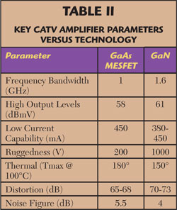
RFMD is currently shipping GaN-based CATV hybrid amplifiers to CATV equipment suppliers in Europe, Japan and North America with volumes greater than 250,000 units shipped today. Operators of hybrid fiber coax (HFC) networks are installing fiber capacity deeper into their networks (“fiber deep” networks) in order to address the increasing demand for higher throughput video and broadband services. GaN CATV hybrid amplifiers provide industry-leading RF output levels, and cable operators using GaN can reduce the number of amplifiers required in emerging architectures and achieve up to 20 percent cost savings in fiber deep networks. The performance of GaN CATV amplifiers is on par with other industry-leading GaAs CATV power doublers but with 20 percent lower current consumption (24 V/380 mA). With these “green” energy-saving benefits, these products enable designers to fulfill growing requirements for lower energy consumption and assist network operators in their drive to reduce the overall cost of operating CATV networks (see Table 2).
Military and commercial radar manufacturers are incorporating GaN-based amplifiers in next generation systems and using similar devices as replacement or field upgrades in deployed systems used in ground based, sea-borne or air-borne applications. The requirement for improved sensitivity, enhanced image resolution, increased coverage and reduction in size and weight are main drivers in the rapid adoption of the GaN-based amplifiers.
Software Defined Radio (SDR) architectures are playing an increasingly important role in emerging radio configurations with requirements for supporting multi-band and multi-standard operation. SDRs have a wide range of applications such as Professional Mobile Radios (PMR) used by law enforcement personnel and emergency responders, military communications (Milcom) such as Joint Tactical Radio System (JTRS), and cellular base station transceivers (BTS). The key enablers for SDR include wideband linear front-end components such as the power amplifier (PA), which are critical to the ability of the SDR to adapt to multiple bands, modulation formats, and radio standards. For systems like the JTRS and PMR, power amplifiers need to operate over multi-decade bandwidth covering VHF, UHF, and L-Bands, and need to be highly efficient and compact, especially when the amplifier is used in a handheld or mobile unit. By using a single wideband PA instead of individual narrowband amplifiers for each band, significant cost savings are obtained. Utilizing a GaN process that is optimized for the best linearity has resulted in devices that provide peak power 30 to 90 W with ability to achieve IM3 better than -50 dBc backed off in power.
Everyday GaN: TriQuint Viewpoint
Dean White, TriQuint Semiconductor, Hillsboro, OR
GaN-based technologies continue to emerge in the global marketplace through new product innovations that span the gamut of consumer, high-performance commercial and defense systems. GaN has proven its frequency, power and wide bandwidth capabilities in applications that range from light-emitting diodes to relatively low-frequency communications and power applications, and to emerging solutions for bio-mechanical/medical applications. TriQuint has focused on high-power/high-frequency innovations that have made GaN technology a mainstay for advanced radar, communications and electronic warfare (EW) programs.
TriQuint Semiconductor began its gallium nitride development in 1999, starting with a combination of government and internal funding. TriQuint’s 0.25 µm GaN on SiC high-power/high-frequency process is ideal for wide and narrowband communications, radar, EW and related applications. More recently, the company’s E/D-mode (enhancement-depletion) GaN on SiC process is seeing increased utilization for contracts that support ambitious programs funded by DARPA and the tri-service laboratories. TriQuint began developing a 0.15 µm GaN process to address emerging commercial and defense millimeter-wave (mmW) applications in parallel with its 0.25 µm DARPA WBGS and Title III programs.
TriQuint sees opportunities for GaN across many different applications from handheld radios to satellites, and from compact UAV radars to large-scale traveling wave tube (TWT) replacements. EW applications such as signal jammers are also a perfect fit for GaN because of the need for high power across broad bandwidths.
Defense communication products benefit from GaN’s ability to provide high power added efficiency (PAE) at high power levels, making the technology suitable for radios operating from UHF to W-Band. At lower frequencies, GaN holds an advantage over LDMOS in that it is much easier to match over several decades of bandwidth. The need to increase the range and capability of UAVs has resulted in a need for smaller, higher power transmitters. GaN is a superior choice because of its high power density and efficiency. Communication systems benefit in prime power and weight reductions enabled by GaN’s higher PAE and compact circuit size at Ku- and Ka-Bands.
Utilizing GaN for radar applications can lead to smaller, higher power radar systems from L- to Ku-Bands. GaN is being used to replace TWTs due to the technology’s ability to offer a smaller footprint and higher reliability. Solid-state GaN power amplifiers have a higher MTTF and require lower cost/less complex DC power supplies when compared to current TWT solutions.
A largely untapped application for GaN is utilization in high dynamic range low noise amplifiers (LNA). With a comparable noise figure (NF) to GaAs, GaN LNAs can provide a low noise figure solution along with higher TOI and higher RF survivability. This allows the selection of lower cost / lower loss limiters where receiver protection is required, since the LNA can tolerate higher RF leakage through the limiter. The utilization of GaN LNAs in some designs may make it possible to eliminate a discrete limiter component. Other areas of interest for GaN technology are found in high dynamic range mixers, RF and DC-DC switches. Advanced high-power, ultra-fast switches are in development for government contracts. TriQuint is exploring ways that GaN will change many ‘everyday’ RF, switch and control product applications for consumer electronics and mobile devices, all the way to satellites.
Specialized for Defense GaN: UMS Viewpoint
Jean Pierre Viaud, United Monolithics Semiconductors, Villebon-sur-Yvette, France
The main initial driver for the development of GaN technologies within UMS is the requirement of the European Defence & Space market for systems offering enhanced performance. This is directly related to the position of UMS as the main European provider of strategic technologies for these applications. In addition to this, the Defence sector particularly has been an early adopter of GaN technology and products for applications in S- and C-Band radar systems for the replacement of TWTs and Si-based HPAs. In the longer term, GaN will enter EW systems offering a greater bandwidth and power capability and active antenna T/R modules replacing both the current GaAs HPAs and LNAs. Prototype products, with state- of-the-art performance, have already been demonstrated for each of these markets, and system evaluations are underway.
In the commercial telecom markets, the push towards broader bandwidths, higher power levels and reduced power consumption will see GaN products being progressively adopted. Applications here will include cellular base stations, VSAT terminal and point-to-point radio links. Of course, it will be essential to fully demonstrate that GaN can provide a solution with the right level of reliability and overall system cost saving to be able to displace existing mature technologies, e.g. LDMOS in base stations.
As well as these classical applications, the inherent power capability of GaN will open up completely new markets, particularly in the industrial area. However, we must keep in mind that the GaN technology is an emerging technology and is less mature and more expensive than GaAs and LDMOS for the time being. Therefore the market penetration of GaN technology is driven by two main aspects:
- System performances which cannot be obtained by existing less expensive technologies
- Cost saving at system level by architecture simplification due to the use of high performances components
UMS launched the development of in-house GaN technologies and products around seven years ago based on a close cooperation with various research labs (IAF and 3-5 Lab) and the support of European, French and German Defence and Space agencies. This activity has been focused on both a 0.5 µm (GH50) and 0.25 µm (GH25) technology on silicon carbide substrates. The former is targeted for the design of lower frequency very high power transistors, whereas the 0.25 µm version is intended for the development of MMIC products with frequency operation up to 20 GHz. The GaN and GaAs technologies are manufactured in the same facility and benefit from UMS’ extensive heritage and background.
The introduction of this disruptive technology will enable companies to reinforce their existing market position in MMIC power devices and foundry services, and also to penetrate new markets through the creation of a brand new family of packaged high power transistors. At UMS, both GaN technologies are reaching the level of maturity required for market introduction. The 0.5 µm technology has undergone extensive reliability testing and is fully qualified (this technology is also being used by NXP to offer power transistor products to the market). The 0.25 µm technology is frozen and qualification has started.
General purpose unmatched power transistors are available for a wide range of applications including: military communication, radar, jammer, commercial telecom, Satcom, industrial sensors with power levels from 15 to 80 W, operating up to 6 GHz. In addition, 50 Ohm internally matched transistors tunable over S- and C-Bands for Satcom and radar applications and available in a fully hermetic metal ceramic package.
The 0.25 µm MMIC technology has now entered the qualification phase. A preliminary design kit including electrical and layout data is available for starting early access foundry cooperation, and has already been successfully used in many European Space and Defence projects. UMS has also developed several MMIC demonstrators on GH25 technology in order to validate the performance of the technology and to allow the release of products, once the qualification is completed:
- X-band PA: 25 W / 50% PAE
- X-band PA: 35 W / 45% PAE
- 6 to 18 GHz PA: 10 W / 20% PAE
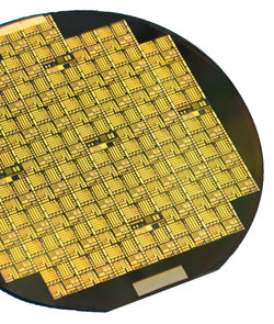
The next steps in the development are planned and include continuous improvement of the production yield and performance of the existing technologies, including the transition from 3 inch to 4 inch wafers.
- Full qualification of 0.25 µm technology and full process release for foundry services
- Space evaluation of GaN technologies
- Release of new power transistors products: 150 W L-Band, 100 W C-Band, 7 W general purpose
- Release of first MMICs: 30 W X-Band, 10 W 6-18 GHz